Relaxation Oscillators
The 555 Timer, Op-Amp Oscillators, the UJT, the PUT, the NE-2 and TTL oscillator packages
The 555 Timer
A relaxation oscillator is a circuit that repeatedly alternates between two states at with a period that depends on the charging of a capacitor. The capacitor voltage may change exponentially when charged or discharged through a resistor from a constant voltage, or linearly when charged or discharged through a constant current source. With exponential charging, the timing is expressed in terms of time constants RC. In a basic circuit, the capacitor will charge with time constant τ1from a starting voltage V1 towards a supply voltage Vu for a time t1. When it reaches some voltage V2, it will then discharge with time constant τ2towards a lower voltage Vd for a time t2, when the cycle will repeat. The period of the oscillator is T = t1 + t2, and its frequency f = 1/T. In terms of these parameters, t1 = τ1 ln[(V2 - V1)/(Vu - V2)], and t2 = τ2 ln[(V2 - Vd)/(V1 - Vd)]. These formulas can be applied to find the periods of the oscillators described below.
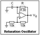
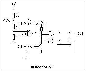 The very popular 555 integrated circuit has everything in it to make a relaxation oscillator. It can detect the voltages V1 and V2, and operate a transistor switch to discharge the capacitor when the voltage reaches V2, turning it off again when the voltage drops to V1. V2 is fixed at 2/3 the supply voltage, and V1 at 1/3 the supply voltage. You can't change these, but you won't want to. These voltages are determined by the voltage divider shown in the diagram, and are detected by the voltage comparators, represented by triangles. The box is a set-reset (SR) flip-flop with complementary outputs Q and Q bar. You have access to output Q, and can get up to 200 mA from it, if you need such a large current. There is a reset pin, that forces the output low when it is grounded, and a trigger pin that forces it high. The threshold input also drives the output high, and this is its normal job.
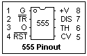 The pinout of the 555 is shown at the left. The pins are numbered in the usual way, starting at the upper left-hand corner, and will be referred to in this way on the circuit diagrams. The maximum supply voltage is 18V, and the maximum power dissipation is 600 mW. The chip will use no more than 12 mA, when there is no load on the output. The rise and fall times of the output are about 100 ns, which is not exactly TTL speed, but should drive digital logic fairly well when necessary without additional help. The CV (control voltage) input gives access to the threshold node, and allows you to filter out any noise by connecting an 0.01 μF capacitor to ground from pin 5. The reset pin, 4, is usually connected to +V when not used, as in most common circuits. Remember that pin 7 discharges the timing capacitor, while pins 2 and 6 detect the upper and lower voltages of a relaxation oscillator. The output is fairly powerful, especially when the supply voltage is 15V, and will supply up to 200 mA. Even at 5V, the 555 will easily drive LED's and small relays.
When the output of the 555 makes a transition, there is a large current spike in the supply current, up to 300 or 400 mA for a short period. For this reason, the power supply should be bypassed with an 0.1 μF capacitor close to the chip.
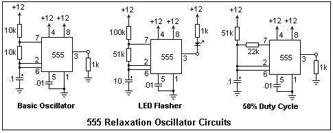
Three oscillator circuits are shown above, and you should try each of them. The LED blinker works slowly enough to be seen, which is the point. One of the bright blue LED's is pretty. The circuit at the left is the usual oscillator circuit, very simple and reliable, but it does not give 50% duty cycle. The duty cycle is the fraction of the period that the output is high, expressed as a percentage. The circuit at the right gives a pretty good square wave, at a frequency of 137 Hz. In this circuit, the resistor in the pin 7 lead must be less than half of the other timing resistor, or the circuit will not reach the lower trigger voltage. If you do not have an oscilloscope, increase the values of the timing resistors and capacitor and use an LED at the output, so that you can see the operation. The scope is better, because you can see the waveform.
Work out the formulas for the periods of the two different oscillator circuits, and check by experiment. For the basic circuit, T = 0.693(R1 + 2R2)C, where R1 is the upper resistor. For the circuit shown, the calculated T is 2.1 ms, and I measured exactly that with the scope! Luck, but these formulas should give accurate results.
There are many 555 circuits, as any application note for the chip will show, and as many uses. There are many "improved" versions, such as the 5555 or 7555 CMOS timer, and many others. The MOS versions have lower leakage currents, and so can be used for longer timing intervals, but do not have as much drive and ruggedness. The 556 is a dual 555 that is useful for those circuits that use two timers. The 555 is really an analog chip, but it looks fairly digital and, as we have mentioned, can interface with digital logic. It will just work on 5 V, but some of the improved versions can use considerably lower supply voltages.
The CMOS equivalent of the 555 is the 7555, which acts in exactly the same way. The 7556 is a dual CMOS timer. These devices have very low input currents at the threshold, trigger and reset inputs, typically no more than 10 pA, compared to the 0.1 μA of the 555. This means that larger timing resistors can be used. However, on 5V the 7555 will only drive 2 TTL loads (-0.8 mA and 3.2 mA). The outputs of the CMOS timers are not nearly as capable as those of the bipolar circuits, which is one thing to watch out for. However, they are equivalent when driving logic.
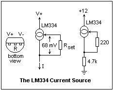 To create a linear ramp that repeats over and over, the timing capacitor can be charged by a current source instead of a resistor. This could be a transistor, but there is a convenient current source in a TO-92 package, the LM334. This device will work over a range of 1 to 30 V (its compliance). The current is set by a resistor connected between the set terminal (R) and the output terminal (V-). The current is about 68 mV/R. A 100Ω resistor gives about 0.7 mA. The voltage stated here as 68 mV is directly proportional to the absolute temperature, varying from about 58 mV at 0°C to 79 mV at 100°C, so the set current varies somewhat with temperature. This means the device can be used as a thermometer, or for temperature compensation, so it is not all bad. The pinout and circuit for this device are shown in the figure. A good two-terminal current source is very useful.
An Op-Amp Relaxation Oscillator
 A classic op-amp relaxation oscillator is shown at the left. The noninverting input is biased at V/2, where V is the output voltage. The inverting input chases this value from below, and when it reaches it, the output voltage changes from one saturation level to the opposite one. The output is a square wave, with a frequency of 1/1.22RC, and duty cycle of 50% if the saturation levels are symmetrical. You can derive this formula easily. With R = 10k, C = 0.1 gave f = 455 Hz, while C = 100 pF gave 289 kHz.
The op-amp indicated, the CA3030, is a MOSFET input, CMOS output op-amp that will swing to the supply rails. The maximum supply voltage for this chip is 16 V, so it cannot be used with a ±12 V supply. I used it with a ±5 V supply. It will also work with a single supply, from +V to GND. Not only will these op-amps work to the supply rails, but their inputs have an extremely high resistance, and the bias current is only a pA or so. The outputs will source 22 mA and sink 20 mA at a minimum, which is excellent. The differential voltage between the inputs must be limited to ±8 V. This specification must be observed with any op-amp in this kind of circuit, where the inputs can be at quite different voltages. Some op-amps cannot be used in this way! The CA3040 is a higher-voltage version, standing a supply up to 36 V, but the permissible differential voltage is the same. CMOS op-amps have some very nice properties, but tend to be electrically fragile, and must be properly treated.
Unijunction Transistor Relaxation Oscillator
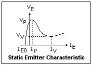 The unijunction transistor, or UJT, is a curious switching device, not an amplifier. It resembles a JFET in that it is a bar of N-type silicon with contacts at both ends, called Base 1 (B1) and Base 2 (B2), and in that there is a PN junction in the middle, with the P silicon connected to the emitter (E) terminal. Current normally passes from B2 to B1, establishing a potential gradient along the bar. So long as the PN junction is reverse biased, nothing much happens; there is just a small leakage current IE0. If you raise the E terminal up in voltage, at some point the PN junction becomes forward biased, and current passes from the emitter into the silicon bar. This injects many holes, which are swept down to B1. The positive charge of the holes calls up an equal and opposite charge of electrons, which drastically lower the resistance between E and B1. The emitter current increases while the emitter voltage falls, which is negative resistance! This means instability, which is exactly what is wanted. The emitter V-I characteristic is shown in the figure on the right.
The resistance between B1 and B2 is called RBB, and the voltage to which the emitter must be raised (the peak voltage, VP) is some fraction η of the voltage from B1 to B2. The UJT I used, a Motorola MU4891, had RBB = 5.53k, and η = 0.66. You will see how to measure η in a moment. If you have a different UJT (practically any will do), be sure about the basing, since it is definitely not standard. In fact, the E terminal is usually at one side, not in the middle, as it is for the MU4891.
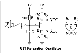 A UJT relaxation oscillator circuit is shown at the left. I used a power supply of 5 V, but it would work just as well (better, actually) at higher voltages so long as the ratings of the UJT were not exceeded. The values shown give a frequency of close to 1 kHz. The frequency is given approximately by f = 1 / RC ln (1/1 - η). The signals that can be picked off at the three terminals are shown, negative pulses at B2, positive pulses at B1, and a sawtooth wave at E. R1 is solely for the purpose of producing output pulses, and can be omitted if they are not required. R2 has the effect of reducing the temperature sensitivity of the oscillator, and has an optimum value for each particular type of UJT. One formula is R2 = 0.7RBB/ηV. The value shown is typical. R and C are, of course, the timing components. If you examine the sawtooth with an oscilloscope, the highest voltage is VP = ηV + VD, where VD is the forward diode voltage, about 0.7 V. This is how to measure η. The minimum voltage is about VV.
The timing capacitor can be pulled up by any voltage, and even by a constant-current source to produce an accurate sawtooth. I found that the capacitor voltage oscillated between 1.3 and 3.8 V, and since it was pulled up to 5 V, I found that the period T = RC ln(2.92) = 1.072 RC, which agreed pretty well with observations. The positive pulse at B1 was 1 V in height, with a rise time of about 500 ns and a fall time of about 15 μs (neither measured very carefully). The negative pulse at B2 was 2.4 V in amplitude, with a fairly quick fall time but it lasted about 28 μs. If your pulse requirements are tight, some pulse shaping will be necessary.
Programmable Unijunction Transistor Relaxation Oscillator
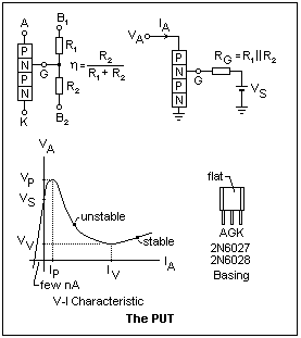 The Programmable Unijunction Transistor (PUT) is not a unijunction transistor at all, but a four-layer PNPN device that can be arranged to act much like a UJT. Its electrodes are anode (A), cathode (K) and gate (G), and the symbol is the same as for the SCR. A voltage VS is applied to the upper N region, which normally reverse-biases the middle PN junction so no current flows from A to K. This voltage is supplied by a resistive voltage divider formed from R1 and R2. The PUT is called programmable because this voltage may be chosen at will, equivalent to changing the standoff ratio η of a UJT. The Thévenin impedance RG of the voltage source determines the electrical characteristics of the PUT.
The VA - IA characteristic shows a negative-resistance region between the peak point and the valley point, so the device can be made to oscillate under the proper conditions. When the anode is made somewhat more positive than VS, the top PN junction is forward-biased, injecting minority carriers into the N region, and causing the usual PNPN breakdown (see the explanation of the SCR). If sufficient current is available, the device operates at a stable point to the right of the valley. For a current of 50 mA, the corresponding voltage is about 0.8 V, and, of course, there is no oscillation.
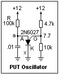 On the other hand, if less than the valley current IV is available, breakdown cannot be maintained, and the device turns off. In a circuit like that shown at the left, relaxation oscillation occurs as the capacitor charges to the peak voltage through resistor R, and then discharges through the PUT. R must be large enough to limit the current to less than IV. In the circuit shown, oscillation will not occur if R is lowered to 68k. The valley current is determined by RG. For RG = 1MΩ, the valley current is about 18 μA, for 10k, 150 μA, and for 200Ω, 1.5 mA. The circuit shown gives a period of 1.26 ms, the output swinging from 0.8 to 8.8 V. The PUT stays ON for about 60 μs before it turns off. Pulse output from the circuit is available at point x in the cathode lead. A small resistor can be placed here for voltage output, or this point can be connected to the trigger of another PNPN device for current output.
The 2N6027 and 2N6028, in TO-92 packages, are manufactured by ON Semiconductors, and are listed as "preferred devices," so they will probably remain available. Data sheets are available on the web at ON Semiconductors. They can stand up to 40 V of either polarity, an anode current of 150 mA, and power dissipation 300 mW.
Capacitance Multiplier
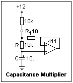 This is as good a place as any to study two curious op-amp circuits, one of which turns a small capacitor into a large one, and the other which acts like a very large inductor. The capacitance multiplier, whose circuit is shown at the right, is useful if you are looking for a long time constant in an RC circuit, and do not have, or do not want to use, a large capacitor. This circuit may help the problem of leakage, at least by permitting the use of a smaller capacitor with low leakage, such as a solid tantalum in place of an aluminum electrolytic. The circuit works by shunting most of the charging current through the small 10Ω resistor instead of the 10k resistor, using the op-amp to sense the capacitor voltage. The multiplication factor is R/R1. I tried it in the circuit shown, for which this factor was 1000, and found that the voltage across the capacitor rose to 8 V in 70 s, certainly longer than it would have been with the 10 μF capacitor in series with 20k, which would give a time constant of 0.2 s. It should have been 1000 s, actually, but I have not investigated the discrepancy, which is probably due to leakage.
P>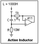 The circuit at the left is an active inductor, and is more complex than the capacitor multiplier. If the output voltage of the op-amp is V', and the voltage at the terminal of the circuit is V, then V' = V[jωCR/(1 + jωCR)], or V - V' = V / 1 + jωCR). Now it is easy to find the input current by adding the currents through R1 and C. The result is I = (V/R1)[(1 + jωCR1)/(1 + jωCR)]. In the circuit shown, CR = 1 s, so the 1 in the denominator is negligible if ω is greater than 10 or so. In the numerator, CR1 = 10, so if ω is smaller than about 1000, then the 1 dominates. Therefore, if ω is between about 10 and 1000, the input current is I = V /jωRCR1, as if the circuit were an inductor of inductance RCR1 H. In the circuit shown, this is numerically equal to R1 in ohm, so the circuit acts like a 1000 H inductor, within the appropriate frequency interval.
Testing the circuit shown is not very easy, because of the high value of L. At ω = 1000 (159 Hz), the reactance is 1 M, so the currents will be quite low with the small voltages available from function generators. I was able to make rough oscilloscope measurements at 10 Hz, and found an impedance of 80k, which is about right for 1000 H. It would be easier to test if R1 were reduced to, say 100Ω or 10Ω.
This circuit taught me a lesson (again) because when I made it, I picked a 51Ω resistor by mistake in the 10M resistor bin without looking at it carefully. Of course, the circuit did not work, and I wondered why. When I made V-I measurements (sensing the current with an op-amp differential amplifier--see the unit on Interesting Circuits), I discovered that the circuit acted exactly like an 0.1 μF capacitor in parallel with a 1k resistance. I went over the analysis of the circuit several times, and even replaced the op-amp in case something was wrong with it. Maybe Horowitz and Hill, the source of the circuit, was erroneous. Eventually, I checked the color code on the resistor and discovered the blue (green, but looking blue in this brand of resistor) was on the wrong end! A real 10M resistor made the circuit work exactly as expected. Analytical errors and approximations, and components, are much more rarely the cause of difficulties than human blundering!
The NE-2
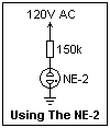 The NE-2 is a venerable cold-cathode gas discharge tube meant for use as an indicator light. It has two parallel electrodes sealed in a small glass envelope with neon gas at from 1.5 to 4.0 mmHg pressure. The discharge "strikes" at about 65 V, then the voltage decreases to about 52 V. The more current that flows, the more the orange discharge glow covers the negative electrode. The NE-2 can be used as a polarity indicator. A few tenths of a milliampere are sufficient to give a full glow. If the current is reduced below a certain level, the discharge is extinguished. The NE-2 must be used in series with some current-limiting device, usually a resistor, as shown in the diagram on the right. Most pilot light assemblies include the resistor. With 120V AC, the NE-2 strikes when the voltage reaches 65V in either half-cycle, and is extinguished when the voltage drops below 52V. Both electrodes appear covered with glow, but a stroboscope will show that they alternate and go out 120 times a second. If you have 240V, just use 330k instead of 150k in series.
When it was realized that glow lamps could be useful circuit elements, General Electric began to manufacture a variety of glow lamps, for circuit use as well as for indicators. Those intended for circuit use had better-controlled characteristics. Most had parallel-post electrodes, wire leads, and a tubular glass envelope ending in an evacuation tip. The envelopes were specified as, for example, T-2, which meant a tubular (T) envelope 1/4" in diameter--the number indicated the diameter in eighths of an inch, a designation that is still used. The largest was the NE-83, 1-1/16" long, with a design current of 10 mA, and intended mainly for voltage regulation. The NE-16 had a bayonet base and "fireman's hat" electrodes. With a design current of 1.5 mA, it was also used for voltage regulation. The NE-77 had three electrodes. The center electrode could be used to trigger the discharge, so that it was a low-cost thyratron. All this wonderful variety of lamps seems to have disappeared, with the exception of the durable NE-2.
There were also Argon glow lamps, with the unique property of being an ultraviolet light source. The AR-9 was a T-2 lamp similar to the NE-2, while the 2 W AR-1 looked like a light bulb, with a medium screw base. Its envelope was designated S-14, and its design current was 18 mA. The AR-3 and AR-4 were similar 1/4W lamps (3.5 mA) with "fireman's hat" electrodes, the AR-3 with a candelabra screw base, the AR-4 with a bayonet base. All neon and argon glow lamps with screw bases, large or small, included a dropping resistor and could be directly connected across 120VAC. The argon lamps were only about 1/3 as bright as a neon lamp, but had the unique property of producing 365 nm ultraviolet ("black light" or UV-A) that was useful in photography and fluorescence. Their light was an attractive violet color. The striking voltage was higher, 90-95 V, and their maintaining voltage was about 70 V.
To determine the resistance of the series resistor in an AR-3 bulb, and the maintaining voltage, connect the bulb so that the voltage across it, V, and the current through it, I, can be measured, using two DMM's. Now measure V for several values of I from about 3 mA down, using an adjustable DC power supply. A straight line, representing the equation V = Vo + IR, should be obtained. R is determined from the slope of the line, Vo from the intercept. This is a simple experiment, but very good practice for a procedure that is often of use. I found R = 12.3 kΩ, and Vo = 71 V. The striking voltage can be found approximately by variying the voltage slowly until the tube fires.
The glow discharge is an interesting phenomenon that has long been studied. Electrons are accelerated by an applied voltage until they gain sufficient energy to ionize the neon atoms, knocking off an electron and forming a positive ion. The ions are accelerated towards the cathode by the same field, and on collision with it cause further electrons to be emitted, which sustains the current. The energy also evaporates some of the cathode material, and "sputters" it onto any surrounding surfaces. At some applied voltage, called the sparking potential, the current becomes larger and self-supporting. The voltage drops, and a glow discharge is established. The ionized and excited neon atoms emit radiation copiously (for neon, at 585.2, 587.6 and 640.2 nm, and other weaker lines in the same region, giving the light its characteristic orange color) in the negative glow, which is what you see in the NE-2. The amount of light is proportional to the current through the lamp.
The random ionization necessary to start the discharge could be supplied by cosmic rays or natural radioactivity in the materials of the lamp, but an important role is played by photoemission caused by ambient light. When a lamp is in complete darkness, the striking voltage rises, sometimes rather impressively. To counteract this "dark effect," some radioactive material may be included inside the lamp. Not all lamps had this modification. If the applied voltage is only slightly greater than the striking voltage, some 200 to 300 μs is required to strike. If the excess voltage is 60-70V, the discharge may form in 25 μs or less. If the discharge has just been extinguished, it may strike again more quickly because of the remaining ionization.
Most of the voltage drop occurs from the cathode to the negative glow, and beyond the negative glow is the Faraday dark (relatively dark) space. If the electrodes are in a narrow tube, most of the region from the Faraday dark space to the anode is filled by the positive column, which glows less strongly than the negative glow, and in which there is a relatively small voltage gradient, just enough to supply the necessary current to the things going on near the cathode. In a neon sign, the positive column supplies the light. The tube is typically 15 mm in diameter, and may be 60 ft long. Typically, the drop is 130 V/ft with a 230-300 V electrode drop, supplied by a 10,000 V (max) transformer at about 25 mA. The higher neon pressure of perhaps 20 mmHg reduces sputtering, which would darken the tube with time.
The NE-2 has no such tube, so there is no positive column outside the Faraday dark space, and the current finds its way to the anode more casually. At one time, there were neon and argon glow lamps meant to work on 120 VAC (there was an internal resistor), about the size of a 25W bulb or smaller, but I have not seen any for a long time. They had an intensity of 0.025 cd/mA, and a surface brightness of 0.8 cd/sq.in., according to one reference. Voltage regulator tubes were larger glow discharge tubes that could supply a reasonable number of mA at 90, 105 and 120 V for a regulated power supply. These, also, have disappeared, along with the need for high-voltage DC plate supplies. They were used like Zener diodes.
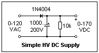 Since the NE-2 requires over 65V to operate, we need a higher-voltage DC supply than the usual 5 or 12 V supplies used with semiconductors. A simple one is shown at the left. A few words about experimenting with 120 VAC: it's safe, but care must be taken. First of all, working with the grounded mains supply is dangerous. Use an isolation transformer to remove this hazard. You don't need much current for most experiments, so even a small transformer is adequate. Wire it up with a cord, switch, fuse and pilot light, perhaps on a wooden base, and use a DIN-style terminal strip covered in plastic (these excellent things are now widely available). I also use a variable transformer so I can use lower voltages when necessary, and test things by bringing up the voltage from zero. It must be remembered that such transformers are autotransformers, and do not solve the grounding problem! Both a Variac and an isolation transformer are necessary. Turn off the power before changing any wiring. Constant awareness will remove most hazards.
Another hazard of higher voltages is capacitors unexpectedly charged. If you charge, say, a 330 μF or other large capacitor to about 50 V, and then discharge it with a shorting wire, you will get a graphic illustration of the power that remains. Discharge capacitors with a 10k resistor to avoid the sparks, and measure the voltage across them. Under a few hundred volts, there is no great problem, but care must be taken. After turning off the power, discharge all capacitors as a regular thing.
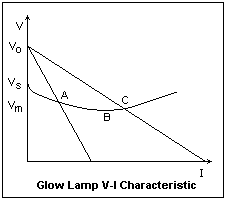 A V-I characteristic for a glow lamp is shown at the left. A striking voltage Vs is required to start the discharge. The voltage falls with increasing current to a minimum at some point B, after which the voltage increases steadily. At some point, off to the right, the discharge changes into an arc, with much larger current and much smaller voltage (which, of course, would destroy the lamp). We recognize the negative-resistance region to the left of B as a region of instability--no point on in can be a stable operating point. Two load lines are shown, one passing left of the point B and the other passing to the right. The operating point C on the right gives normal steady behavior, but the operating point A on the left is unstable. Any slight change drives the operating point to the boundaries of the region, and the tube oscillates between extinction and full conduction. With a 100V supply, a 150k resistor gives an operating current of about 0.3 mA for the NE-2, its normal operating point as an indicator. On the other hand, a 1M resistor produces operation in the unstable region. A capacitor in parallel with the lamp will then make a good relaxation oscillator. Several examples are given below. In the stable region, the NE-2 is equivalent to a 5.5k resistance in series with a 55V potential difference, shunted by 0.5 pF. When extinguished, it is equivalent to an 0.5 pF capacitance. Note that this equivalent circuit does not apply in the unstable region.
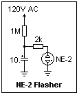 An NE-2 flasher for 120 V is shown at the right. With a 1M resistor, it flashes about every 10 s, and you can follow the voltage changes with a DMM. A 330k resistor will give a period of about 2.6 s. A smaller resistor cannot be used because the current will not fall below the extinction value, and the NE-2 will simply stay on. This, of course, is another relaxation oscillator, which depends on the difference between the striking and extinction voltages of the discharge. If the extinction and strking voltages are V1 and V2, the period is T = RC ln[(Vo - V1)/(Vo - V2)], assuming that the discharge takes negligible time. The 2k resistor is to limit the discharge current and extend the light pulse.
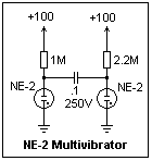 A simple bistable oscillator or multivibrator using NE-2's is shown at the right. The supply voltage is not critical--it works fine on 100 V, and nothing would be wrong with 170 V. The large resistors ensure that the currents are small. They may be 1/4 W, but the voltage rating of the capacitor should be high enough. This circuit oscillates at about 2 Hz, giving the impression of a flickering candle when the bulbs are close together. When using the NE-2 as an oscillator, the important thing is the difference between striking and extinguishing voltages.
The use of glow lamps as voltage regulators is similar to the use of Zener diodes and VR tubes (which are just glow discharges themselves). There is little choice of voltage (55 V for neon) and the current is small (less than a mA for the NE-2), but they are very cheap. The NE-16 and AR-1 give more current.
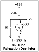 Voltage-regulator tubes (see Vacuum Tubes) are available in some variety, and can be used to make relaxation oscillators. An example is shown at the right. The 0G3 is an 85 V regulator that comes in a 7-pin miniature package. The cathode is connected to pins 2,4 and 7, while the anode is connected to pins 1 and 5. In this circuit, the tube fired at VH = 116 V and extinguished at VL = 72 V. As usual, the anode resistor cannot be too small, or the tube will remain on. The discharge time was small, so the output waveform was a series of rising exponential charging ramps. The period can be estimated from the relation T = RC ln[(VS - VL)/(VS - VH)] = 3.9 ms for the values shown. VS = 125 V.
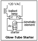 Small glow lamps are used as automatic fluorescent lamp starters. The starters are easy to disassemble. The circuit is shown at the left. The added element is a bimetallic strip that puts a short between the electrodes when it is heated sufficiently. When the lamp is turned on, there is sufficient voltage to strike the discharge, and soon the bimetallic strip completes the circuit through the thermionic filaments f, f'. This extinguishes the glow discharge, and the bimetallic strip cools. When it breaks the circuit, the inductive kick due to the ballast inductor is enough to strike the mercury arc in the lamp. The lamp voltage is too low to maintain the glow discharge, so the circuit stays open. Should the lamp not light, the cycle is repeated. The discharge strikes at about 110 V and maintains at about 81 V in the example I studied. If a 47k resistor is used in series, the approximately 2 mA of the normal discharge provides insufficient heat to operate the bimetallic contact, and the tube can be used like an NE-2. The blue glow means that the gas is probably Argon, not Neon, as in an NE-2, however. The mercury arc in the lamp produces copious short-wavelength ultraviolet that excites the phosphors in the inner wall of the tube. Positive ion bombardment keeps the cathodes hot. The discharge extinguishes and restarts every cycle in alternate directions, at a voltage lower than required for the cold tube, or for the Argon glow discharge.
Crystal Oscillator Modules
 If you need a square wave at TTL levels in the range 1 - 66 MHz, the easiest solution is a quartz crystal oscillator package. The pinout is shown at the right, and is the same for the oblong and square packages. Pin 1 is identified by the sharp corner. The power supply is 4.5 - 5.5 VDC, and the output goes from below 0.5 V to above 2.4 V, with rise and fall times of about 10 ns. The output will drive 10 TTL loads. These packages fit in a DIP socket, and are very easy to use, besides being cheap.
Conclusion
We have studied several kinds of relaxation oscillators in this chapter, but this by no means exhausts the subject. We will see further relaxation oscillators in other units, made from digital integrated circuits, vacuum tubes, and other amplifying devices. There are many other kinds, and some that are not even electronic. There are even biological relaxation oscillators. All include this idea of switching between two semistable states, or bistability. Another name for such oscillators is multivibrator, since their output is rich in harmonics, not a single frequency. The 555 can be used to make circuits that only change state once, to give a time delay, for example, or a single pulse of a particular length. These monostable circuits are useful, but not as interesting as an oscillator. There are also oscillators that are not relaxation oscillators, and these have many useful properties and are very interesting. Such linear oscillators may have difficulties starting and in limiting their amplitude, problems that do not occur with relaxation oscillators.
Return to Electronics Index
References
AR-3 lamps are available from Sunray Lighting, Inc., 1 Whatney, Irvine, CA 92618-2806 for about $8.25, plus handling and postage. They are called "J2A" lamps.
Composed by J. B. Calvert
Created 21 July 2001
Last revised 17 August 2002