In digital systems, a limited number of circuit states, usually two in the nearly universal binary logic, contain the information, instead of the continuously variable information in an analog signal. The science of digital logic is presented in texts and courses in Digital Design, to which the reader is referred for a great deal of interesting information, most of which is not used in practical work, at least not any more. Here, I want to discuss mainly the electronic or circuit aspects of the integrated circuits used in digital devices, which is of great utility in practical work. We will not be very interested in the information carried by the digital signals.
There are two kinds of digital integrated circuits in common use. There are more varieties, some quite esoteric, but these two handle most of the load, and are the only ones easily available for study and use. The two kinds are bipolar ("TTL") and CMOS, and both are about as old as integrated circuits themselves. Their circuit properties are quite different, although modern devices can actually be used together (this is not usually a good practice, however). Bipolar devices, somwhat inappropriately called TTL (transistor-transistor logic), early became the most popular choice, together with NMOS large-scale devices that imitated TTL properties. CMOS with its rugged flakiness was used when power drain had to be kept to a minimum, and for certain devices where its peculiarities were valuable, as in ripple counters and the 4046, for example. The TTL integrated circuits were given numbers 74XX, while the CMOS circuits had numbers 4XXX.
The two states of TTL logic were a low state near 0 V produced by a saturated transistor switch, and a high state of rather indefinite voltage, provided either by a pull-up resistor, or by the "totem-pole" output of a circuit, which pulled up the output near 5 V. These two states are very easily distinguished, and insensitive to noise, especially the low state. The effect of noise depends not only on the voltage outputs, but on the output resistance as well, so comparison of voltage levels is not a reliable guide. 4000 CMOS suffered from high output resistance and high input resistance as well, which allowed small extraneous charges to cause problems. However, the saturated transistors of TTL took a lot of current, and also a lot of time to get out of saturation (though they were much faster than CMOS).
TTL was modified by a Schottky diode between collector and base that prevented transistors from going into deep saturation, saving both current and time. The circuits were also redesigned to use less current, and were called LS, or low-power Schottky. The numbers were now 74LSXX. There have been further developments (e.g., "fast" or 74FXX, "low-power" or 74LXX, "Schottky" or 74SXX--same power as TTL but much faster, etc.) but LS is excellent, inexpensive and superior for general use.
CMOS was also greatly improved by giving the outputs a lower resistance, and making the circuits work more like TTL. The result was the 74HCXX series, which has the same functions as TTL, even the same pinouts, and can replace LSTTL in most applications. There is a variation in which the inputs are made to mimic TTL inputs, called HCT, with part numbers 74HCTXX. These work reliably when LSTTL outputs are connected to their inputs, while HC might not. Otherwise, they have no advantage over the normal HC chips, which should usually be chosen. Although HC chips resemble TTL in look and function, they are true CMOS, with the peculiarities of that family.
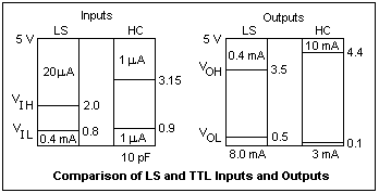
HC (or HCT) outputs can drive up to 10 LSTTL inputs. Even 4000-series CMOS can drive 2 LSTTL inputs. A CMOS output swings from near the supply to near ground, so will be properly interpreted by any logic input. With a 4.5V supply, the HC input logic levels are H > 3.15 V and L < 1.35 V, whereas the LSTTL and HCT levels are 2.0 V and 0.8 V, respectively. The CMOS input current is guaranteed less than 1 μA, but is typically a tenth of that or less. Some input current is required to charge the input capacitance of about 5 pF, but this will have little effect.
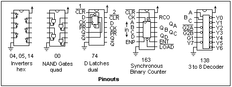
The arrangement and pinouts of the chips we shall exercise here are shown in the figure below. The symbols for inverters and gates will be familiar. An open circle represents logic inversion, but really a pin that is "active low," that is, performs its function when pulled low, while its normal state is high. This usually has nothing to do with digital logic, and is a pure circuit function. The power connections for all these chips is in the standard "corner" positions, pins 14 or 16 for +5, and pins 7 or 8 for GND. The 14-pin and 16-pin packages are standard for LS and HC digital logic circuits.

It's important to understand the characteristics of the inputs and outputs of the LS and HC families, which are quite different. The HC family is in many ways simpler, since the inputs carry only a very small leakage current, less than a microampere, no matter what is done to them. They have a capacitance of 10 pF, which governs the amount of charge that has to be moved to change their states. The outputs provide ("source") current when high, and accept ("sink") current when low. When high, they act like a small resistance connected to the positive supply, and when low like a small resistance connected to GND. The small resistance is around 50Ω, and the high and low states are relatively symmetrical. An HC output can be made to give or accept 20 mA, though this is something of a strain. They will easily drive an LED at 10 mA or so whether high or low.
An LS input handles current. When you hold it high, it wants something around 20 μA, and when you pull it low, you have to accept 0.4 mA. If you leave the input disconnected, or "open," it can't get the current it wants at any voltage, and acts like a high or H state. For experiments, one can simply leave unused inputs alone, and they will act as highs. In actual circuits, it is best to connect unused inputs to +5 or GND by wires. Some people use 4.7k resistors instead of a plain wire to pull up inputs, but it really doesn't make much difference with LS. With HC, inputs MUST be given a definite state. If left alone, they will float to some intermediate value and now be one thing and now another. In 4000 CMOS, they put things in an intermediate state where the circuits drew excessive power. With HC, I have not noticed this, but the uncertainty of state still remains. When experimenting with HC, it is good practice to wire all unused inputs to +5 or GND.
An LS output is also different from an HC output. It pulls up to something over 3.5 V, but usually not to +5 if there is any load at all. Most LS chips give around 4.7 V when high. In this state, it will not furnish more than about 0.4 mA without dropping below 3.5 V. The pull down is quite different. Here the output will absorb up to 8 mA without rising above 0.5 V. This is the advertised value, and most chips will do even better. There is no problem sinking 20 mA if you can stand the output voltage's rising a bit. (the HC's output will be up to 1 V by this time). The output is, therefore, asymmetric, as are the inputs. One LS output will handle about 20 LS inputs, as far as static current is concerned. The characteristics of LS and HC inputs and outputs are compared in the figure below.
The number of HC inputs that can be supplied from one HC output (the "fan-out" as it was once called) is not limited by current, but by capacitance and the speed required. 10 HC inputs have about 100 pF capacitance, and the output has a resistance of about 50ω, so the time constant is 5 ns, which is fast enough for most purposes. The inputs of both LS and HC do not like voltages that change too slowly. A rise time of over 500 ns can lead to problems, especially with complex chips. Although we study these chips with DC voltages, they are actually high-powered racing cars, not family sedans, and require special handling if they are to work at their accustomed speed.
The rise and fall times of inputs and outputs should not be confused with the propagation time of a signal across the chip from input to output. Propagation times for inverters are 15-20 ns for either LS or HC, which is fairly typical of digital logic.
The supply voltage for LS is 5.00 V (4.75 V to 5.25 V), and must be held within this range by a properly-regulated power supply. A 5.1 V Zener can be used for this purpose. The supply voltage for HC is much more flexible. It can be anything between 2 and 6 V (7V is the maximum, and it is not good to shave this too closely). It works satisfactorily on 3 V, but is normally used with the same 5 V supply as for LS. HC draws very little operating current when operating at slow speeds, only microamperes, so it is the obvious choice for battery-powered devices.
These investigations used HC devices. They can be repeated with LS devices as well, for a comparison between the two families. The first step is to look at the output voltage as a function of the output current, for both the high and low states of the output. Incidentally, a current into a device (sunk) is shown as positive, and one out of a device (sourced) as negative, in data sheets, but just positive values are used here.
Study one of the six inverters in a 74HC04 hex inverter package. Connect the inputs of the other five inverters to GND. Connect the input of the inverter under study to GND, and measure the output voltage with the DMM. Now connect load resistances of 10k, 1k, 470 and 100 successively, from the output to GND, measuring the output voltage each time. Now connect the input to +5, and repeat the measurements, connecting the load resistances to +5 in this case. Sketch the output voltage as a function of current in each case, and estimate the output resistances. I got 48Ω for H, and 35Ω for L. Remember that actual chips are usually better than the guaranteed specifications in data sheet.
The next step in the usual school lab is to vary the input voltage while monitoring the output of the inverter to find the point at which the transition is made. This is not really a well-defined point, but rather a region in which a rapidly changing input triggers the change, so it is much better to find this point dynamically than with a static input. If you do not have an oscilloscope, you should do it statically, and find that LS changes at about 1.0V, and HC at about 2.5 V.
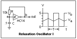 The circuit at the right is a relaxation oscillator, using a 74HC14, an inverter with a Schmitt trigger input. This means that the transition point for an increasing input is higher in voltage than the transition point for a decreasing input. The difference is called the "hysteresis." Such an input is very useful for a slowly-varying input or one with noise, since once a transition is made, the opposite transition will not occur immediately. That is, the input will not "bounce" or chatter. Such an input is required for this circuit to work, and the transition levels will be displayed on the oscilloscope. The capacitor voltage oscillates between the upper and lower transition levels, which for the HC14 are typically 2.0 and 3.0 V and vary with the supply voltage. These values may vary considerably between different chips, so an oscillator must be hand-adjusted to produce a certain frequency. Also, the duty cycle is not exactly 50%. Look at the waveforms until you understand what is going on. This circuit will not work with a 74LS14, because the inputs load the RC circuit too heavily. You will note a little "ringing" at the top of the rising transition of the output.
Digital logic inputs are meant to be connected directly to digital logic outputs, without discrete components in the circuit. Since HC input currents are so small, this requirement can be eased, as in these relaxation oscillators. However, it should be remembered that digital logic IC's are not operational amplifiers, and cannot be used in the same ways.
The time between each transition is the same going up or down, and is t = RC ln 1.5 (the equation to solve is 5 - 3 exp(t/RC) = 3), so the period T = 0.811 RC or f = 1.233/RC. This gives f = 1233 Hz for the given circuit, and the measured value was 1440 Hz, which is reasonable agreement.
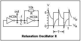 Another relaxation oscillator, operating on a different principle, is shown at the left. It is not necessary to use a Schmitt trigger input for this circuit, so the standard inverter, the 74HC04, is shown. The idea here is to slow down the changes to the input of the second inverter by using an RC circuit. Its output is connected to its input, so it has no stable state. In the waveforms, note that the capacitor voltage relaxes towards zero until it reaches the transition point at 2.5 V, then the voltage is reversed and it charges towards 2.5 V. The maximum voltage on the capacitor is greater than the supply voltage, here about 6 V. This gives t = RC ln 2.5, or f = 1/2t = 0.545/RC Hz. The calculated value for this circuit was 545 Hz, and the measured value was 541 Hz. The frequency of oscillation can be varied over a wide range by changing R and C, well into the MHz region. These oscillators work best for HC, since the outputs swing all the way to the supply rails, but will also work with LS.
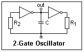 The preceding oscillator can also be drawn as at the right, where an additional resistor R2 has been added, as seen in a National Semiconductor Application Note (88) on CMOS logic. Without the capacitor, this would be a bistable circuit, as is any ring of an even number of inverters. In fact, this circuit may not oscillate for certain values of C. However, it normally does, as we saw in the last paragraph. The duty cycle is only about 66%, but the waveform at the output node is a reasonable square wave.
This oscillator has R2 = 0. Note that R2 is in the input to a CMOS inverter, so the current through it will be practically zero. This means that the value of R2 will have no effect on the frequency, which can easily be verified by experiment. I found that for 10k, f = 538 Hz, for 100k f = 533 Hz, and for 1 M, f = 503 Hz. Finally, for 10 M, the frequency dropped to 383 Hz, since the input currents are actually in the microampere range. In Application Note 118 on CMOS oscillators, a formula for the frequency of a similar oscillator is given that actually includes R2! It is strange that this application note seems to have been dry-labbed and published.
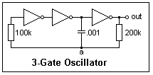 This circuit is shown at the left. Since there are three inverters in the loop, it will always oscillate, and generates a good square wave. Its frequency does not depend on the value of the resistor shown as 100k, despite its appearance in a formula given in the application note. I measured a frequency of 2328 Hz for the values shown. Its frequency is pretty well given by the same formula as for the two-gate oscillator above.
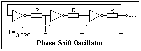 Another kind of CMOS oscillator is shown at the right. It is a loop of three inverters, so will always oscillate. Without the RC components, it would oscillate at a very high frequency (MHz) depending on the propagation delays of the inverters. At some frequency, the RC branches give a phase shift of 60°, so the overall phase shift will be 180°, and the circuit will oscillate at this frequency. With R = 330k and C = 0.001 μF, the oscillation frequency was 918 Hz. The waveform was approximately sinusoidal, and its peak-to-peak value was 6.5 V with VDD = 12 V. For these circuits, I used a CD4049, but an HC inverter would work as well. More relaxation oscillators are studied in the page devoted to them.
The next circuit to be studied is the 74HC00 quad NAND gate. This is a typical logic gate, giving an output that is a Boolean function of the inputs. A NAND gate outputs 0 (low) when both inputs are 1 (high), otherwise 1. It is called positive logic when 1 is associated with the high voltage state, and 0 with the low voltage state, and this is the usual convention. It is, however, the voltage relations that are basic, not the logic name. With negative logic it becomes a NOR gate, giving 1 (low) when both inputs are 0 (high), otherwise 0. NAND, NOR, AND, OR and XOR gates are available with various numbers of inputs in great variety. Complex functions are no longer assembled from discrete gates, except for small circuits or unique functions. However, gates are still very useful, especially the simpler ones.
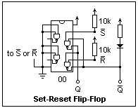 The circuit at the right is a set-reset flip-flop, or SR FF. Notice the feedback between the two gates, which gives it two stable states, in one of which Q = 1 and /Q = 0 (the bar over the Q is represented by a slash in text). This is called the set state. In the other, Q = 0, /Q = 1, and it is called the reset state. Which state is set and which reset depends purely on which output is chosen to be Q, and it not fundamental. Trace the states through the gates to verify these statements. The inputs marked /S and /R are pulled up with resistors, and can be pulled low by touching the nodes with a wire connected to ground. When you touch the /S node, if Q = 0, then both inputs were 1, but now one of them is 0, and this causes the output of this gate to go to 1. The feedback makes both inputs of the other gate 1, so its output goes to 0, and the circuit is set. Touching /R with ground has the same effect, on the other gate, and causes the circuit to be reset.
If you touch /S twice, or more, rapidly, the second touch apparently has no effect, since the first one set the circuit. Whenever you make a connection like this, by manually touching a wire, or by any kind of mechanical switch or relay, you often get more than the one touch you expect. The contacts "bounce" for a period of milliseconds, making and breaking repeatedly. Normally, this is no matter, but with digital electronics it certainly is. A digital circuit will register each bounce as a separate pulse. A counter, for example, will make multiple counts (we will see this later). If you need a single pulse or edge (an edge is a step increase or decrease), it cannot be done with a switch or wire. The SR FF can be used to "debounce" a contact. If you do not have a debouncing circuit set up permanently on your breadboard, then use the one you have just made for the later parts of this exercise. You can continue to use a ground wire to tap /S and /R, or you can connect an SPDT pushbutton to do this much more easily. From now one, I will assume that you have a debounced pushbutton and can make single rising or falling edges when you want them.
A variable-frequency oscillator made from a 4001 CMOS quad NOR gate is shown in the page on Analog Delay Lines. The older 4000-series CMOS can take higher supply voltages than the HC series, up to 15 V. A clock signal of 12V amplitude is required in this page, so the 4001 is used. The inputs of the NOR gates are connected together, so the result is effectively a simple inverter, but this is merely for convenience, and there is no necessity for using NOR gates. Just as the 7400 quad NAND was the basic TTL gate, so the 4001 quad NOR was the basic CMOS gate.
The 74HC74 is a dual D-type latch. A latch is a more complicated circuit, made up from gates, that serves to store a digital value. This latch has complementary outputs Q and /Q, like the SR FF, a /CLR control that resets the latch to Q = 0, and a /PR (preset) control that sets the latch to Q = 1. Data (a 1 or a 0) that you want to store in the latch is applied to the D or data connection. Finally, a rising edge applied to the CLK (clock) input causes the value currently at D to appear at Q. This happens only in a very short interval around the edge. After the edge is gone, no changes to D have any effect on Q. Such a latch is said to be edge-triggered. The value does not actually appear at Q until the input is no longer sensitive, so it is easy to make a toggle by feeding Q back to D. Now the latch will toggle, that is, a 1 will become a 0 or a 0 a 1, every time there is a positive edge at CLK.
Take a 74 and wire it up for testing. Refer to the pinout above, and use the latch on the left, No. 1. There is another one whose pins are on the right-hand side. Since we will not be using it, wire each of its inputs (everything but Q and /Q) to +5. On the left, pull up D, CLK, /CLR and /PR with 10k resistors so you can operate them by touching with a ground wire. Connect an LED with 330Ω series resistor to /Q, so that LED on = set, LED off = reset. Apply power, and test the /CLR and /PR controls first, which reset and set the latch, respectively. They act at once, and are called asynchronous because of this. Put values of 0 and 1 on D, and tap the /CLK node with a ground wire, to make first a negative edge, then the active positive edge. You will see that D is transferred to Q each time, and that Q changes only when /CLK tells it to.
Now connect D and /Q. This should make a toggle flip-flop, or T FF. When you try it however, sometimes it works and sometimes it doesn't (you may be lucky, but that is a rare gift). The reason, of course, is bouncing, where you get two or three toggles for each touch. Connect CLK to the output of your debouncing circuit that is normally low. Now when you press the pushbutton (or touch /S) you will get one and only one edge, and the T FF will work perfectly. A T FF divides a frequency by 2, providing a 50% duty cycle at the same time, which is often useful.
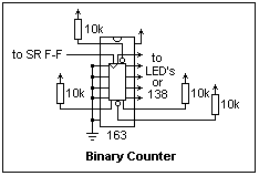 The next circuit is really a very complicated one, internally, but its use is fairly simple. It is one of a family of 4-bit counters, made up of flip-flops and gates. Nobody makes counters from discrete gates and flip-flops any more. It is a binary counter, meaning that the outputs are bits with weights 1, 2, 4 and 8, and it counts 0000, 1000, 0100, 1100, 0010, ..., 1111 in 16 steps, and keeps repeating. The low-order bit is on the left here, and the high-order bit is on the right (oppositely to the way a binary number is usually written). Let's call them A, B, C and D. The output changes for a positive edge on the CLK input, so this counter is edge-triggered, like the 74. There are inputs for the ABCD values, as well as outputs, called QA, QB, QC and QD.
There are also /LOAD and /CLR controls. As might be expected, /LOAD loads the values at the inputs ABCD into the counter, and they appear at QA, QB, QC and QD. /CLR clears the counter to 0000. On this counter, these controls are synchronous, which means they take effect only when there is a simultaneous positive edge on CLK>. Connect +5 and GND to the chip, pull up /CLR, ENP, ENT, and /LOAD with 10k resistors, apply any values you like to ABCD, wiring them to +5 or GND, and connect CLK to the debouncer. I have LED's on my breadboard driven by inverters, so I can connect the outputs and RCO to them to display the state of the counter. I recommend using LED's to show the output state highly, so you can immediately see the count. If you connect them directly, they will show 0 states by being on, and the chip really was not intended to drive LED's (use as low a current as you can if you connect LED's directly). The counter should count in this state, increasing one step for each clock edge. Prove to yourself that /CLR and /LOAD only work when you also bump the clock. It is good to understand clearly the difference between synchronous and asynchronous events.
People usually want to count higher than 16, so multiple counters are used. The RCO output, and the ENP and ENT inputs are used for this purpose. For synchronous counters, the same clock is applied to each chip, and you have to keep the higher-order counters from counting until it is time. To do this, the 163 provides an RCO output, the ripple carry out. This is connected to the ENT input of the next higher counter. Since ENT must be high to count, and it is usually low, the next counter does not count. When the count reaches 1111, RCO goes high, the next counter is enabled, and registers a count with the next clock pulse. ENT and ENP differ only in that ENT also enables RCO, while ENP has no effect on RCO. For further information, consult the data books and texts on digital design. Both ENP and ENT must be high to count.
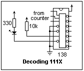 The final example is a 3-to-8 decoder chip, the 138. This takes a three-bit input, ABC, and causes a different output to go low for each of the 8 possible input numbers from 000 to 111. It will give us something to do with the outputs of the counter. Let's set it up to detect when the output bits are 111X, that is, 1110 or 1111. This corresponds to the output labeled Y7, if ABC are input to the pins so labeled on the 138. The 138 has three enables, G1, /G2A and /G2B. Wire up the chip as shown, and connect ABC with the corresponding outputs of the counter. Make the counter count, and watch the result. Modify the circuit so that the LED lights only for 1110, not for 1111. Now modify it so that it detects 1111 (like RCO) but not 1110. This will show how to use the enables of the 138.
Both the HC outputs, and the totem-pole outputs of LS, actively pull the output towards +5 or GND. This means that we cannot connect two outputs together, since if the logic states were different, the outputs would contend for superiority, and the issue of the match might be uncertain. However, there are many situations in which we want to connect outputs together, most importantly to create a bus that carries different information at different times, as in computers, where busses are essential. For this reason, tri-state outputs are offered in both HC and LS. These outputs have an enable control that switches them from being effective, and driving the bus, to exhibiting only a high impedance, as if disconnected. The three states are H, L and Hi-Z. When enabled, these outputs act normally.
An alternative is the open-collector bus, which still offers certain advantages. The outputs that are to be connected to this bus have no active pullup. They only sink current, towards ground. They are the collector or the drain of a transistor, and are called open-collector or open-drain outputs. Such outputs are also ideal for driving LED's, and other loads that do not require pull-up, and for loads which pull up to a higher voltage than the logic supply. An open collector can switch loads to, say 30 V, which is impossible for a totem-pole or tri-state output. The gate symbols show an open collector output by drawing a transverse line near the output end.
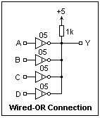 The HC05 is open drain, and the LS05 is open collector. The diagram shows four open-drain inverters connected to a bus pulled up by a 1k resistor. This connection is called a wired-OR because the result is low only if one or more of the inverter outputs is active. Outputs in opposite states do not contend in this case.
The TL507 is an obsolete I2L-technology (Integrated Injection Logic, a bipolar process that was briefly popular) package that was once available from Radio Shack. It is an interesting little 8-pin DIP that provides a good exercise in digital logic, and also solves a problem of some difficulty quite neatly, that of creating a square wave of easily variable duty cycle from 0% to 100%. Look it up on the Texas Instruments website. A link is provided in the References.
What it contains is a counter that starts at 127 and counts down to 0 at the command of a TTL clock signal on pin2. The maximum clock frequency is about 125kHz, which means the counter can count all the way down in about 1 ms. The binary digits of the counter are weighted inputs to a summer, so a voltage slope is produced that begins at 0.75 V+ and ends at 0.25 V+. For 5 V, this is from 3.75 V down to 1.25 V. The output of the summing op-amp is one of the inputs of a voltage comparator, while the other is the input voltage Vin. When the counter begins at 127, the output is high (it is an open-collector output, and must be pulled up to the logic voltage, which can be anything up to 18 V.). When the ramp voltage becomes less than the input voltage, the output goes low.
The way this chip is used to generate a square wave of variable duty cycle should be clear. The output is high 100% of the time for Vin < 1.25 V, and is high 0% of the time for Vin > 3.75 V. The input frequency is divided by 128 in the process, so we can make a square wave of variable duty cycle up to 1 kHz in frequency. The chip can accept from 8 to 16 V on pin 7 as the positive supply, called VCC2, which is internally regulated to the operating voltage, or 5 to 6 volts on pin 6, which is called VCC1. If 5 V is supplied to pin 6, pin 7 can be left open or connected to pin 6. The conversion is relative to the voltage at pin 6, so it is called ratiometric. Each count corresponds to (0.75 - 0.25)VCC1/128 V. With VCC1
= 5.12 V, each count is 20 mV. If the input voltage is less than 200 mV, the output goes low automatically.The chip really can do a more elegant job: it can convert an analog voltage to a binary number. Binary numbers are mainly of interest to computers, and with a computer, it is easy to use the TL507. You simply send a tick on the clock line, and check to see if the output went low. This is done over and over until the output finally does go low, while you count the number of ticks. This would be very boring for a person, but for a computer it is a piece of cake. The TL507 (while it existed) was probably the cheapest way to get a conversion, and the speed was adequate for many applications (such as temperature control). However, for us at this point it forms an intellectual exercise: can we make a standalone analog to digital converter, such that when we press a button, the binary number corresponding to the voltage is displayed?
What has to be done is to make a counter count in unison with the TL507 while it is counting, and to stop the count when the output goes low. Pressing a button should reset the counter to 0 and the TL507 to 127, releasing them when you raise the button. The controls we have on the TL507 are the reset RST at pin 8, resetting when high, and enable EN which must be high to count. When EN is low, everything stops, and the output goes high (unfortunately). If you don't take some decisive action, the TL507 just goes on counting.
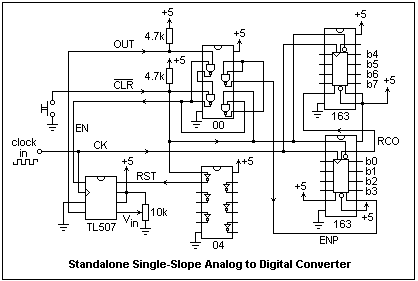 My solution uses a set-reset flip-flop, with the two states count and pause. Count is set by pressing a button which controls a /CLR signal, while pause is set by the output's going low. While the button is depressed, the TL507 should be reset and the external counter also brought to zero. The circuit is shown at the right, with all the pins of the chips shown pictorially, to make it easier to wire the circuit. It is a bit complicated, but that is the way with digital circuits. The bit outputs of the counters can be displayed with LED's; I have an octal HCT buffer on my breadboard for the purpose. It is worth it to see the lights flicker. Instead of a pushbutton for /CLR, I just used a wire that I touched to ground to start a conversion. Of course, it seems instantaneous if the clock frequency is high enough. Vary the voltage and record the binary output from the external counter. It really works quite well! I was a little disappointed by having to use the 74LS04 inverter. Can you find a simpler circuit?
There are very many ways to do analog to digital conversion, and this is only one method. A/D conversion is a study in itself, more closely related to computers and digital electronics than general electronics. There are tradeoffs of speed and accuracy, and many details to arrange, to achieve good results.
The traditional symbols with distinctive outlines for gate functions and simple rectangles with labeled connections for more complicated circuits are used here, and seem still to be common practice. Nevertheless, IEEE Std. 91-1984 specifies different, international symbols developed by the IEC (International Electrotechnical Commission) in the early 1970's. This system has some merits, but is essentially a solution without a problem, and rather too complicated. I have seen it used only in data books and such, and it may be used by the more authoritarian institutions that like such things. Most engineers are familiar with the properties of the limited number of available packages, and there is no need for the symbols to express them. Certainly, the existence of an elaborate symbolism is no aid to design, which depends on knowledge of individual properties.
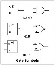 Symbols for NAND, NOR and XOR gates are compared at the right. The IEC symbols still use the inversion bubble in some cases, but the slanted line as seen on the outputs of the NAND and NOR gates is more common, and specifically indicates a low level, rather than a logic 0 or 1. Positive logic, one will recall, uses the high state for logic 1 and the low state for logic 0. The basic symbol is a rectangle, with the function expressed by a qualifying symbol like & for AND and ≥1 for OR. XOR is simply =1, since the output is one only when one or the other input is one. Inputs are on the left, outputs on the right. When this rule is violated, arrows are used to show the direction of signal flow. The slanted lines showing inversion may be used on inputs as well as outputs, where they look like half-arrowheads.
 Qualifying symbols within the outline are used at inputs and outputs; some are shown in the figure. The right-pointing triangle means the outputs have more drive than usual, as the LS38 for example, as compared with the LS00. A triangle with the point downwards means tri-state output. There will be an input labelled EN which is the enable. If it is active low, it will have the slanted line, as shown. An open collector or drain output is shown by a diamond on a horizontal line. An input with hysteresis, a Schmitt trigger input, is shown by a small hysteresis symbol. There are many more of these, but these are the most common ones.
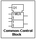 The only distinctive outline used is the common-control block, shown at the right for an imagined dual one-of-two data selector, for which the qualifiying symbol is MUX. The address input G1 at the top acts for both data selectors, selecting one input when 1, the other when 0.
The triangle to show an edge-triggered input, as on a D flip-flop, is used in the IEC system. A T by the triangle means an edge-triggered toggle. D identifies a data input, while J, K, R and S have the usual meanings relative to flip-flops. A binary grouping of inputs is bracketed, and labelled 0 and m on the extreme inputs, where m is the highest power of 2. With this information, you should be able to figure out most symbols for the usual logic chips. Nothing at all has been said about the dependency notation that expresses the logical connections between inputs. For this elaborate system, one must refer to the standard itself. It is interesting, but I believe it to be of very little use, a mere bureaucratic exercise. Some Texas Instruments data books give an introduction to the IEEE Std. 91 symbols.
Don Lancaster, CMOS Cookbook (Indianapolis, IN: Howard Sams, 1977) and TTL Cookbook (Indianapolis, IN: Howard Sams, 1974) contain explanations, data and circuits that are an excellent introduction to digital circuits, and may still be available.
The Texas Instruments website has technical information available on the TL507, and much else besides.
Composed by J. B. Calvert
Created 26 July 2001
Last revised 7 August 2008