Switching Regulators
The LM2576, LM2577 and LM2574 make it easy to build buck and boost switching regulators
Introduction
Switching voltage regulators work by periodically storing energy in the magnetic field of an inductor, and then discharging the energy into the load. This is a reversible process, so there is no essential energy loss, as there is in the familiar linear voltage regulator or dropping resistor. They can transform the input voltage into a higher, lower or negative output voltage. There is a large selection of integrated circuits containing a switch and the circuits used to control it, which make the construction of a switching regulator very easy. We shall use the National Semiconducor SIMPLE SWITCHER series of integrated circuits, which have current capacities of 5, 3, 1.5, 1 and 0.5 ampere, using the 3 A versions as examples. Full information can be obtained from the National Semiconductor website cited in the References.
 Suppose we have a load that requires 5 V and draws 1 A, but we have only a 12 V supply. The simplest solution is shown in the diagram at the left, the use of a dropping resistor, here of 7Ω. Note that 5 W is dissipated in the load, but 7 W in the dropping resistor, so the efficiency of this arrangement is 5/12, or 42%. Normally we are not concerned with the cost of such a small power loss, but the heat that is produced can be a problem. In this case, we must use a rather large power resistor, not a small 1/4 watt part.
Maintaining these values also depends on the constancy of the supply and the load. If the load should draw less current, then the voltage supplied to it will rise, ulitmately as far as to 12 V, and if it draws more, then the voltage supplied to it will decrease. Dropping resistors are only practical when the load is constant (as it often is in electronics, explaining their poplarity). If the supply voltage changes, the output voltage will change proportionately, in this case by a fraction 5/12. Changes in the output voltage resulting from supply or load changes is called the regulation. The load regulation is usually defined as the percentage change in the output voltage between no load and full load.
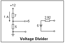 Regulation is better in the case of load or supply changes if we use a voltage divider, as shown in the diagram at the left. The internal resistance of the resulting source will be rather low, so the output voltage will not change much with a change in load (Thévenin's Theorem). However, the efficiency is even lower than with a dropping resistor. Normally, we should only draw a current that is much smaller than the current in the divider, here 1 A, so the output power will be much smaller than the power dissipated in the divider. Nevertheless, voltage dividers are often very useful.
The solution to regulation problems is the use of a feedback regulator. The output voltage is compared to a reference voltage, and the error signal is used to control the output voltage. In a linear regulator the control element is, in effect, a variable resistance, such as a series bipolar transistor or MOSFET. Power must be dissipated as with a dropping resistor, so there is no increase in efficiency. Linear regulators have been discussed in Experiment 11.
This experiment studies a different kind of feedback regulator, the switching regulator, that makes use of an inductor to change the voltage, instead of a resistor. The energy loss of a dropping resistor is eliminated, so thermal matters are very much simplified and the efficiency is high. Many integrated circuits have been designed to realize switching regulators. Only a few easy-to-use IC's are mentioned here. Switching regulators can also be step-up or produce a negative voltage, which linear regulators cannot match.
Stability considerations are important with any feedback circuit, and switching regulators are no exception. Circuit designers make this as easy as possible for the user, so in many cases it does not need to be explicitly investigated. Generally, switching regulator circuits are stable if the capacitors are large enough, as will be mentioned below. In most practical cases, the capacitors are considerably larger than required for stability.
Switcher Circuits
There are three types of switcher regulator circuits. The buck circuit produces a voltage less than that of the supply, the boost circuit produces a voltage greater than that of the supply, and the negative boost circuit a voltage opposite in sign to the supply. A linear regulator can only produce a voltage less than that of the supply, but a switching regulator is much more flexible. We shall see that it is very much like a DC analogue of the AC transformer.
Each of these circuits contains an on-off switch that we will consider ideal in the explanations. In practice, the switch is usually a bipolar transistor, so in the ON state it has the saturation voltage drop, normally about 1 V, in which power can be lost and heat produced, reducing the efficiency of the circuit. There are two general ways to control the switch. In one mode, the time the switch is ON is constant, but the frequency of ON pulses varies. In the other, the switch is turned on at a fixed frequency, but the time it is ON is varied. We shall use this pulse-width modulation (PWM) mode here, since it is used in the LM2576 IC.
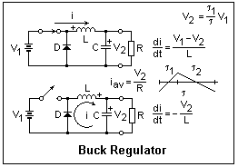 The buck regulator circuit is shown at the right in its two states, with switch closed or open. The output voltage V2 is less than the supply voltage V1, so that when the switch is closed, current flows in the direction shown, opposed only by the inductive reactance of the inductor L. The diode is reverse-biased by V1 and does not conduct. Therefore, the current increases at a constant rate di/dt = (V1 - V2)/L and additional energy is stored in the magnetic field of the inductor. This happens in the same way whatever the initial current in the inductor. The average value of this current is the load current I2 = V2/Rload.
The current is allowed to increase during a time τ1, after which the switch is opened. Now the diode is forward-biased, since the voltage across the inductor is larger than V2 as it strives to keep the current flowing by using the energy stored in its magnetic field. The current decreases at a constant rate -V2/L for a time τ2, when the switch is again closed. In a steady state, the increase must be equal to the decrease. By equating these changes, we find that V2 = (τ1/τ)V1, or that the output voltage is the duty cycle τ1/τ, where τ = τ1 + τ2.
The switch control samples the output voltage and compares it to a reference voltage. If is is too high, the pulse width must be reduced, but it it is too low, the pulse width must be increased. This automatically holds the output voltage at the desired level. It might seem that the circuit would work without the capacitor, but the capacitor is necessary for the stability of the feedback loop.
Let I1 and I2 be the average input and output currents. The output current is constant, but the input current pulsates. Since there is, ideally, no energy loss, V1I1 = V2I2, or I2/I1 = V1/V2, just as in an ideal transformer. In a switching regulator, the input current is not equal to the output current, as it is in a linear regulator. For a step-down regulator, the current taken from the supply is less than that delivered to the load, a rather desirable feature. Even better, there is no large amount of power to dissipate with the associated thermal problems. Also, it is very easy to vary the output voltage, usually by only rotating a potentiometer.
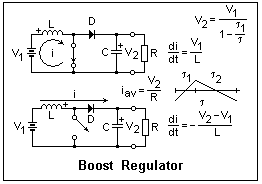 The boost circuit is shown at the left. When the switch is closed, the diode is reverse-biased by the output voltage, while the load is supplied from the capacitor. The supply "charges up" the inductor, starting from the average current. When the switch is opened, the inductor is placed in series with the supply and provides enough extra voltage to drive current into the capacitor against the output voltage V2, which is clearly greater than the input voltage V1. By equating the current rise and fall, we find that V2 = V1/(1 - τ1/τ). In principle, V2 can be varied from V1 to infinity by changing the duty cycle. The average output current I2 is now less than the input current I1.
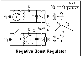 The circuit at the right shows how to obtain a negative output voltage from a positive supply. The positions of the inductor and the diode are interchanged with respect to the buck regulator. When the switch is closed, the diode is reverse-biased and the load is supplied from the capacitor, as in the boost circuit. When the switch is opened, the inductor must drive current into the capacitor in the direction shown, with the diode forward-biased. In this circuit, the supply is never directly connected to the load, and supplies all the energy through its magnetic field. The inductor is switched between the supply and the load while carrying a current that varies only a little up and down. The output voltage as a function of duty cycle is shown in the diagram, and may vary in principle from zero to negative infinity. This circuit is also called a buck-boost circuit.
The LM2576 Switching Controller
The LM2576 includes a switch, voltage reference and feedback path for use in either the buck or the negative boost circuits. It has a capacity of 3 A, and a maximum supply voltage of 40 V, or 60 V in the high-voltage LM2576HV version. Feedback resistors may be included for output voltages of 3.3, 5.0, 12 or 15 V. The -ADJ version uses external feedback resistors and can be adjusted to any output voltage. The switch saturation voltage is typically 1.4 V and is responsible for most of the power dissipation. A heat sink may be required, but the thermal dissipation is internally limited. The input voltage should be 12 V or more. The quiescent current is typically 5 mA, or 50 μA in standby (on/off high).
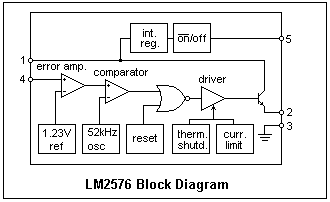 A block diagram of the LM2576 is shown at the left. The oscillator frequency is nominally 52 kHz (τ = 19 μs), but may vary between 42 and 63 kHz. This frequency makes the use of fast-recovery diodes essential. The 1N4000 series has a recovery time of about 2 μs, as can easily be measured by testing a diode in series with a 1k resistor. They are not satisfactory as the catch diode in a switching regulator. Schottky (metal-junction) diodes are much faster, with a scarcely perceptible recovery time in the same circuit. The lower ON voltage is also an advantage. The voltage rating should be at least 1.25 times the maximum input voltage. The circuit is supplied in a TO-220 package with five leads, as illustrated below. It also comes in other packages, including the metal TO-3 case.
 A circuit for testing the LM2756 is shown at the right. The electrolytic capacitors at input and output should be connected with leads as short as possible. The voltage rating of the capacitors should be comfortably higher than the voltages used in the experiment. The load of 100Ω is rather light, so power dissipation will be small and not troublesome. A heat sink is not required in this case. The diode is a 40V, 1A Schottky diode; the 40V, 3A 1N5822 should be used for heavier currents.
The inductor sizes used in a switching regulator make a ferromagnetic core convenient. Since such a core is subject to saturation, it must be designed to retain its inductance in the presence of a DC current. Such inductors are called chokes. The inductor shown is a Jameco 371670 of 330 μH that is rated for 1.7 A. Since we are using only small currents in this experiment, it will be satisfactory. The Jameco 371418 is 220μH, and can handle 3.6 A, so it would be satisfactory for higher currents. The inductor is chosen to keep the current ripple below a few percent of the average current. The data sheet gives design guidelines for inductor choice.
There are two requirements on L. It must be large enough to ensure loop stability, and its value determines the ripple in the output current. In most cases, the second requirement governs. The choice of L depends on two parameters. One is denoted E·T, and is the voltage applied to the inductor times the time it is applied, which is the duty cycle times the oscillator period. This equals LΔI, since E = L(di/dt). The other is the average inductor current, I. Therefore, ΔI/I = E·T/LI, which seems to be taken as about 1/4 in the data sheets. This gives L = 4E·T/I, in μH if E·T is expressed in V-μs. The next larger standard value of L should be chosen. This is equivalent to using the charts in the data sheet. A larger value does little harm, if it is convenient or smaller ripple is desired. The inductor must have a DC current rating equal or greater than the current I to avoid saturation.
 The voltage divider in the feedback loop is designed to give 1.23 V when the output voltage is at the desired level. In this case, when all the 2k potentiometer is in, the output voltage will be 1.23 x 3 = 3.69 V, so the output current will be about 37 mA. The minimum output voltage will be 1.23 V. The feedback bias current is only 50 nA, so the feedback divider is very lightly loaded. With a supply of 40 V, a larger potentiometer (say, 50k) would give a variable voltage supply from 1.23 V to about 35 V, very convenient in the laboratory, and not accompanied by the large power dissipation of a linear regulator. A suggested ripple filter is illustrated at the right; it should reduce the 52 kHz ripple by about a factor of 1/200. The inductor must be a choke rated for the DC current.
The output ripple is mostly the voltage drop in the equivalent series resistance (ESR) of the output capacitor due to the current pulses, not simply the change in capacitor voltage due to a change in charge. Heat is also produced by this drop, which may overheat the capacitor. It may be necessary to choose low-ESR or low-impedance aluminum electrolytics if this heating is troublesome. Higher voltage rating capacitors usually have a smaller ESR. Choose the voltage rating of the output capacitor as at least 1.5 times the output voltage. For stability, Cout > 13,300 (VI/vOL) μF, where L is in μH. Cout should be greater than 100 μF in any case.
The circuit was assembled on a solderless breadboard. Alternate leads of the LM2756 were bent backward and forward, and then down and carefully twisted by 90° so they could be pressed easily into the board. A 12 V laboratory supply was used to energize the circuit, and the output voltage was displayed on an oscilloscope as well as measured by a DMM. The voltage ripple was only millivolts, but with the typical brief switching transients on turn on and turn off. The output voltage was very easily adjustable within the range possible. The lower feedback divider resistor should be a minimum of 1k, the recommended value. The output voltage remains steady when the supply voltage is varied, but the length of the ON interval decreases at higher supply voltages, as expected. The input and output currents can be measured with two DMM's, which allows a determination of the efficiency, which should be greater than 75%. Subtract the quiescent current from the input current before calculating the efficiency.
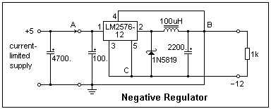 The LM 2576 can create a voltage below ground from a supply voltage above ground. The circuit is shown in the diagram at the left. The inductor is switched between the input and ground, as in a boost regulator. Note carefully the ground connection and follow it from left to right. The trick that allows the feedback loop to work as usual is to "bootstrap" the ground pin of the LM2576 to the negative output voltage. The IC effectively works between the + input and the - output. The absolute value of the negative voltage can be greater or less than the positive input voltage. This circuit is only a slight modification of the buck circuit described above. There are circuits where the LM2576 works completely below ground, but these are not really very useful.
If you use a power supply with current limiting to energize this circuit, it probably will not start. There is a heavy current drain on starting that will cause the supply voltage to fall below what is necessary to cause switching to start. To overcome this, use a large capacitor as shown. Turn the supply on first, then make the connection at "A". The capacitor will hold the voltage up so that switching can start and the output capacitor can be charged. If you use a normal linear supply without current limiting, this will not be necessary.
This circuit can be changed to a normal buck regulator simply by removing the connection at "B" and connecting it at "C". This can be used to check that the circuit is wired correctly.
The dropout voltage is the minimum voltage difference between input and output at which the regulator will function properly. For the LM2576, the dropout voltage is about 1.5 V at an output current of 3 A, and often less than 1 V for smaller output currents.
The LM2577 Switching Controller
The LM2577 is similar to the LM2576, but is used in the boost circuit, where it switches the input to ground. One application is producing +12 V from a +5 V supply. It has an RC compensation network that is not necessary with the LM2576. It will work down to 3.5 V input voltage (unlike the LM2576), and the switch can stand 65 V. Like the LM2576, its oscillator frequency is nominally 52 kHz, and the switch transistor can carry 3 A. A large output capacitor is necessary for loop stability. Note that Vin, pin 5, powers the chip, while Switch, pin 4, is the input to the switch.
 A boost circuit using the LM2577 is shown at the right, which produces 12 V from a 5 V supply. The 17.4k resistor is a 1% value to produce an accurate 12 V output, but for testing purposes it can be replaced by any convenient value, such as 18k, or by a potentiometer to produce an adjustable voltage. A 25k potentiometer would work very well and allow adjustment from 5 V up to 16.6 V. Note that a boost circuit cannot produce a voltage less than the supply voltage, since then the diode would be permanently forward-biased. The load shown is rather light, but good enough for testing purposes. The data sheet suggests that this circuit will supply up to 800 mA. The load would then be 15Ω, 12W, which would require a power resistor. When constructed with a feedback divider of 18k and 2k, the circuit supplied 12.54 V from an input of 5 V or 7 V. Of course, the input voltage should have no effect on the greater output voltage.
The data sheet gives formulas for choosing the values of Rc and Cc. Rc should be less than 750Iload(VO/VI)2, and in any case less than 3k, for stability. Cc should be greater than 58.5(Cout/Vc) (VO/Rc)2, but in any case greater than 0.22 μF for proper functioning of the soft start circuit. This circuit prevents a large current inrush when the regulator is first turned on.
The output capacitor Cout should be greater than either 0.19LRcIload/(VIVO) or VIRc(VI + 3.74 x 10⁵L) / 487,800VO3. In all these formulas, volt, ohm, ampere, henry and farad are the units.
The selection of the inductance L is a little more complicated. L is between 47 μH and 2200 μH, with the larger values for the smaller load currents. A minimum L is necessary for stability. This value is 6.4(VI - 0.6)(2D - 1)/(1 - D) μH, where D is the duty cycle. The maximum duty cycle is D = (VO + VF - VI)/(VO + VF - 0.6). VF is the forward voltage of the catch diode, 0.5 V for a Schottky diode. This value of L is usually small, and so L can be chosen to reduce the ripple to a reasonable value. Graphs are given in the data sheets for the choice of L on the basis of ripple current, as described for the LM2576, which is normally a few hundred microhenry.
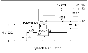 An interesting circuit that should be mentioned is the flyback regulator, shown at the left. Note the characteristic transformer, with a divided secondary. The polarity dots are shown on the windings. An increasing current entering at any dot causes current to enter the other dots. When the primary is connected between the supply and ground, the diodes prevent any current from flowing in the secondary. The primary then acts like a simple inductor and a magnetic field is established. When the switch opens, the collapsing field causes currents in the secondary that forward-bias the diodes and charge the output capacitors. Feedback is taken from the positive output. Although an LM2577-12 is shown, an -ADJ could be used for any desired voltage, within limits. The difficulty is obtaining the flyback transformer, which is not available at Digi-Key, Mouser or Jameco. Transformers are often used in connection with switching regulators. Because of the high frequency, the cores may be small and light, unlike those used at 60 Hz.
The LM2574 Switching Controller
 The LM2574 is used just like the LM2576, except that its maximum current is 500 mA. The oscillator frequency is 52 kHz, as for the LM2576. It comes in an 8-pin DIP, which is possible because it does not dissipate much heat, as a linear regulator would. Pin 5 is the input, and pin 7 the output. Feedback is brought to pin 1, which the circuit tries to maintain at 1.230V. Pins 2 (signal ground), 3 (on/off) and 4 (power ground) are grounded. Pins 6 and 8 are no connection, but soldering them to the circuit board helps to dissipate heat. A typical buck circuit is shown above. The 10 Ω resistor is the load, drawing the maximum rated current of 500 mA at 5 V. The feedback resistors set a nominal voltage of 5.04 V. The circuit can be powered by a 12 V, 300 mA wall transformer as indicated. When the output current is 500 mA, the input current is only 250 mA, giving an efficiency of 83%. This is easily observed on test, showing how a switching regulator is like a transformer.
Of course, a 78M05 linear regulator could be used instead, but the output current would only be 300 mA if this were the capacity of the wall transformer, and a good deal of heat, requiring a heat sink, would be generated.
References
J. Stewart, Build a Switching Regulator, Nuts and Volts Magazine, June 2008, pp. 42-46.
LM2576 and other data sheets can be downloaded from Jameco . All the components necessary for this experiment can be obtained from Jameco. Digi-Key handles a wider variety of National Semiconductor products.
Data sheets and other information can be found at National Semiconductor.
P. Horowitz and W. Hill, The Art of Elecronics, 2nd ed., (Cambridge: Cambridge University Press, 1989), Chapter 6, Sec. 6.19, pp. 355-368. Includes an excellent description of computer switching supplies, which avoid a heavy power transformer and a lot of heat, but are complex.
Return to Electronics Index
Composed by J. B. Calvert
Created 8 June 2008
Last revised 25 July 2008