Interesting Circuits
Follower, differential, common-base, cascode, shunt-series pair and complementary pair
Followers and the JFET
A follower is a circuit in which the potential of the output tracks the potential of the input--an amplifier of unit gain. Usually, the benefit is that the input of the follower has a high input resistance, while the output of the follower has a low output resistance. Feedback is the perfect way to get this, and the proper configuration is the series-mixing, shunt-sampling which, we know, raises the input impedance and lowers the output impedance. However, to study followers we do not need to use feedback concepts, but can proceed directly from fundamentals. Nevertheless, feedback will give us extra insight.
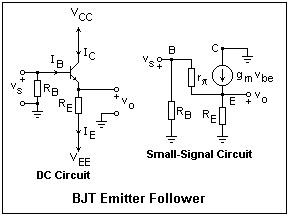 A bipolar junction transistor, a BJT, is an excellent amplifier for a follower; the circuit is shown in the figure. A bipolar power supply (this bipolar has nothing to do with the transistor's bipolar) is shown, with VCC positive, and VEE negative. There is an emitter resistor RE which sets the bias current, and provides the feedback. Since the emitter terminal will be at about -0.7V with the input grounded, it is easy to find the required value of the resistor when the desired emitter current is known. The emitter current only differs from the collector current by the small base current, which is less than 1% of the whole, so usually we neglect the difference, as it will not have any practical effect on our analysis. The base resistor RB is there only to provide a path to ground for the base current. It is actually an annoyance otherwise, lowering the input resistance. It can be as large as 1/10 of the resistance looking into the base of the transistor and have a negligible effect on the bias. An AC input can be coupled with a capacitor (not shown), and an AC output can also be taken through a capacitor, to avoid disturbing the DC bias.
Construct a follower using a 2N4124 or similar npn transistor, VCC = - VEE = 12 V, RE = RB = 10k. Measure the emitter and base voltages, and from them find IC, IB, β, gm and re in the usual way. If you connect the base resistor to the wiper of a potentiometer instead of to ground, you can watch the output voltage follow the input as you vary it. The output voltage will always be about 0.7 V below the input, of course. If you really need a DC follower with no offset, this can be done, but it is not necessary for an AC follower, which will be capacitor coupled anyway. For this circuit, the resistance looking into the base will be about 1.7MΩ (so the base resistor could be a lot larger), and the output resistance will be about 19Ω. These values are so large and so small, respectively, that they are difficult to measure accurately. A BJT makes an excellent follower!
The small-signal equivalent circuit can be used to find the AC properties of the follower. Neglecting the base current, we can write vo = ieRE = gmRE(vs - vo). Solving for vo, we find that vo/vs = RE / RE + re, where we have used the fact that re = 1 / gm. This, of course, is just our feedback loop calculation, and the result shows that the follower has a sort of voltage-divider property. It should also be clear that the output resistance is just the parallel combination of re and RE. If we had gone to the effort of considering the difference in the collector and emitter currents, the only effect would have been to multiply re by β/(β + 1).
Now couple a 1 kHz signal into the base with an 0.1 μF capacitor. Calculate the corner frequency of the resulting RC high-pass circuit, and note that it will not attenuate the input. Set both scope probes to AC, and look at the input an output. You will be able to superimpose them, nearly. The output is just like the input, and that is what you want. I found a gain of essentially 1.0; the calculated value was 0.998. You can load the circuit with a 10k resistor to ground, coupled with another 0.1 capacitor. It will take some effort to see any effect, with such a low output impedance. Note that the low output impedance does not mean that the follower will supply any current you want--it's limited by the emitter current's going negative to about a milliampere. So, we couldn't hang a 1k load on the output, for example, and expect the follower to feed it.
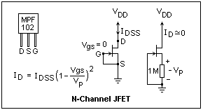 Let's look at another kind of three-terminal amplifier, the junction field-effect transistor, or JFET. This is the kind of amplifier that everyone was looking for without success when the BJT was discovered. An N-channel JFET is just a piece of N-type silicon through which the current passes from one end to the other. The ends of this channel are called drain (D) and source (S). The drain is usually positive, and the source negative, but the two terminals are really pretty much the same electrically. Nevertheless, it is a good idea to operate with the drain positive because the transistor is optimized for that polarity. There are also P-channel JFETS, that work the same way, except that now drain and source are exchanged, and the source is positive. In the symbol, the little arrow points the other way. This arrow is usually drawn on the source side of the transistor in either case. Just as for BJT's, the symbol is drawn upside down so current still goes from top to bottom in the circuit diagram.
The third terminal is the gate (G), which is the control terminal. It makes a PN junction with the channel, and when it is reverse-biased (as it always must be!) the depletion layer eats into the channel and takes away the charge carriers, raising its resistance. In fact, the JFET can be used as an electrically-controlled variable resistor, but we shall not use it this way here. When the gate is sufficiently negative (in the N-channel JFET) the channel is cut off. The voltage for this is called VP, the pinchoff voltage, and is negative for an N-channel JFET. If the channel is pinched off from end to end, things are a bit boring. However, if it is pinched off only at the drain end, then it acts like a constant-current source controlled by the gate voltage. The drain current in this case more or less follows a simple quadratic law, which is shown in the figure. The two parameters are VP and IDSS, the drain current with gate and source at the same potential. The figure shows how to measure the necessary parameters with your meter. JFET's are notoriously hard to manufacture according to strict specifications, so you can save money by buying a type that is not selected to meet particular numbers. For example, the MPS102 can have IDSS anywhere from 8 to 20 mA,and VP anything less (more positive) than -8 V. Find a JFET and measure its VP and IDSS. Mine had -3.8 V and 12.2 mA, respectively. The values of VP and IDSS usually track.
A formula for the transconductance, gm = dID/dVGS can be found by differentiating the equation for ID. One such formula is gm = 2ID/(Vgs - VP). The denominator is the positive difference between the two voltages--how close it is to pinchoff. My JFET gave 2.71 mS, a good deal less than the 59.6 mS for a BJT at the same current. JFET's are not nearly as good as BJT's at amplification, and are used only when their specific properties are useful. The most important of these is that the gate current is practically zero. There is some gate current, the leakage across the PN junction, but it is very small. Nevertheless, it must have a path to ground or the JFET will not work.
 A JFET follower is shown in the diagram. Note that the supply voltages are now labeled VDD and VSS, and the nodes D, S and G rather than C, E and B. The leakage gate current is actually in the other direction from the arrow. The small-signal equivalent circuit of a JFET follower is much like that of a BJT follower, but even simpler since the base or gate current does not have to be considered at all. For signal purposes, the gate is an open circuit. The formula for the gain is the same, with RS replacing RE and rs ( = 1 / gm) replacing re. Since rs is larger than re, a few hundred ohms instead of a few tens or less, the gain is noticeably less than 1.0.
Build a follower using the same values as for the BJT, except that RG should be 1 MΩ. An even larger value could be used successfully, but then measurements with the multimeter would have to be corrected for its input resistance. The input coupling capacitor can be reduced to 0.01 μF, accordingly. I found a gain of G = 0.905 and an output resistance of 593 Ω. These are about what was expected, but more care would probably produce better agreement. The formula for the transconductance is only approximate, and this parameter could be measured directly for greater accuracy. The DC offset between input and output was much larger than for the BJT, about 2.73 V, the bias necessary for the bias drain current. This problem of DC offset also has a solution, but it involves another transistor as a reference. JFET followers can be made with wonderfully high input resistances (the gate resistor has to go!) and this is one of their major uses, in which no other device can do so well. Many op-amps now have JFET input stages.
Note that there is no collector resistor in these circuits. The input is into the base, but the output is taken from the emitter. In the small-signal circuit, note that the collector is at signal ground (that is, its potential does not vary with the signal), and is common to input and output. For this reason, a follower is often called a common-collector amplifier. The familiar transistor amplifier with output from the collector is a common-emitter circuit. You are correct if you assume that there is also a common-base amplifier configuration. The only reason it is not more widely used is its low input resistance. However, this is not a drawback for a current amplifier, and common-base amplifiers are often found in this application.
Differential Amplifier
Before getting into differential amplifiers, let's review small-signal transistor models, and introduce a new one that will be of service. In the figure below, the new model is on the right, and our familiar models on the left. The resistances rπ and re both are related to how much the output current changes with respect to input voltage, and the relations of them to the general parameter, the transconductance gm, are shown. Once you know the bias collector current, you can calculate these important parameters.
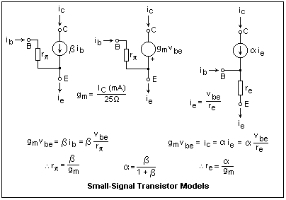
In the new model, which we may call the alpha model, the direct connection of the base may worry you. However, note that the current-controlled current source in the collector makes sure that only the proper base current flows. In the (good) approximation that α = 1, there will be no base current at all. The connection to this internal, inaccessible node is only to put the base-emitter voltage across the resistor re to make the emitter current. The collector then takes what it likes, leaving the rest for the base. In fact, alpha is often taken as unity when you use the alpha model for quick insight, for which it is specially adapted.
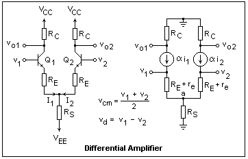 A differential amplifier is shown at the right. There are two inputs and two outputs, and the circuit is assumed to be symmetrical, which it always is in practice, to a first approximation. If only one output is used, the other collector resistor can be eliminated, with no change to the functioning of the circuit. It is very convenient to express the inputs as the sum of a common-mode input vcm, which is the average of the two input voltages, and the differential mode input vd. In the common mode, the same voltage vcm is applied to the two inputs. In the differential mode, opposite and equal voltages &plusmi;vd are applied to the two inputs.
In the common mode, the amplifier acts as a single amplifier with collector resistance RC/2 and emitter resistance RS + (RE + re)/2, so the gain (the ratio of the resistances), input impedance and output impedance can easily be found, as for the single-transistor amplifier. If the input is taken single-ended, the gain is RE/(2RS + RE + re). RS is usually made very large, so that the common-mode gain is small. In many cases, RS is actually replaced by a current source that has a very high internal resistance, so the common-mode gain is practically zero. This means that the amplifier will not respond to any signal common to the two inputs, which is generally desirable.
In the differential mode, the symmetry of the inputs means that node "a" will not change in voltage, and i1 = -i2 = vd/(2RE + 2re). From this result, the gain at an output node is easily found: G = RC/2RE + 2re). This is called the single-ended gain. If the output is taken between the two collectors (double-ended) the gain is twice this value. Note that we have inverting and noninverting outputs as well as inputs. The differential input simply divides the same total current between the two sides of the amplifier. It can go no farther than to put all the current through one collector or the other, however.
Consider a circuit in which the input is to v1, the other input grounded, and the output is taken at vo2, with RC1 removed. Then we have an emitter follower driving the collector of the second transistor, which forms a common-base (this input is grounded) amplifier. This circuit is good for very high frequencies, for reasons that we shall explore elsewhere. This circuit uses feedback, of course, though we did not use feedback analysis.
Construct and test a differential amplifier using RC = 4.7k, RE = 470Ω. Choose RS so that the collector current in each transistor is about 1 mA, and use a ±12V supply. The single-ended differential gain should be about 5, the common-mode gain about 0.5 and the input impedance at one input about 100k. (How did I get these numbers?). The actual differential gain is a little smaller than 5, because the current source for the emitters is not a good one. The input source can be a buffered potentiometer.
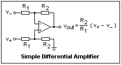 A differential amplifier can be constructed using an op-amp, as shown at the right. An op-amp is a differential amplifier itself, but its gain is far too high and frequency dependent to be used as such. The inverting and noninverting inputs are shown by v- and v+. The formula for the differential gain is easily obtained by considering the noninverting input grounded, which means the op-amp tries to keep both its inputs at zero, so the feedback on the inverting side is like a lever with lengths R1 and R2 (since the same current flows in both resistors, of course). The common-mode gain is easily seen to be zero, since the inputs go up together if the output voltage is zero. Of course, the actual common-mode gain will not be zero because of various small inequities, both in the resistors and in the op-amp. I tested such a circuit with a 411 op-amp, using R1 = 10k and R2 = 100k, for a differential gain of 10 (20 dB). Using 5% resistors, the common-mode gain was 0.029, and with 1% resistors, it was 0.019. The common-mode rejection ratio, CMRR, was, therefore, 10/0.019 = 526 or 54 dB.
If you put a 100Ω resistor between the input terminals of the amplifier I tested, the result is a current sensor with a sensitivity of 1 V per mA that can be used to observe the current at any point with an oscilloscope, which must sense with ground as one terminal. The differential amplifier removes this limitation, which is often quite annoying.
Common-Base and Cascode Amplifiers
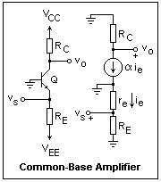 A common-base amplifier is shown in the figure. A bipolar supply is used so that we can simply ground the base, without having to use the extraneous voltage divider that would be necessary with a unipolar supply. It's not a very mysterious circuit; the output is still taken from the collector, as usual. The input, however, is presented to the emitter. The resistor RE is required for bias purposes, and is not a feedback resistor as in most previous circuits. The small-signal emitter current is negative (this is just a change; the DC emitter current can't be negative, of course), and equal to vs/re. The alpha model is very convenient here. Now we can find the gain, which is G = RC/re. Note that the gain is positive, and can be large, because of the smallness of re. The input resistance is a bit less than re (actually re in parallel with RE, and so is quite small. A small resistor in series with the emitter will help to lower the gain and raise the input resistance. If you need a low input resistance to terminate a transmission line (say, 50Ω), a common-base amplifier is just what you want.
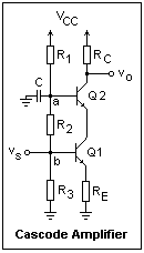 We have just seen that a differential amplifier can be considered as an emitter follower driving a common-base amplifier, the emitter follower providing the desired low output impedance. The base can also be driven in another way, by the collector of a current source with very high internal resistance, and this circuit is called the cascode, which is shown in the diagram at the left. Q1 acts as a voltage-controlled current source here. The output resistance of a transistor is 100k or greater, so it makes a good current source, even if the collector voltage is varied, that does not require a lot of supply voltage (as a large resistor would, for the same current). This current is then injected into the emitter of Q2, which simply passes it along, since alpha is practically unity. The base of Q2 is grounded for signal purposes by the capacitor C. The collector voltage of Q1 is equal to the voltage at node "a" less the base-emitter drop of Q2. This clamps the collector voltage of Q1, making it a very good current source indeed, with an output resistance of many megohms. The voltage gain of the circuit is seen to be about -RC/RE, since RE is again a feedback resistor. The only defect is the voltage divider used to get the correct bias voltages on the bases of the two transistors, which lowers the input resistance and requires a large value of C. The reactance of C at the lowest signal frequency should be lower than the resistance looking into the voltage divider at that point (with the base disconnected), so node "a" will be held near ground. The cascode is another circuit that has a wide bandwidth.
Build and test a cascode amplifier using RC = 4.7k, RE = 1k, and a collector current of about 1 mA. Design the voltage divider to provide the required voltages, with the divider current swamping the base currents that will be about 10 μA. Make the emitter voltage of Q2 sufficiently higher than the base voltage of Q1 that Q1 will not be saturated. A power supply of 12V should be just sufficient, but will not allow a very great output swing. You can couple an AC signal into the base of Q1 with a capacitor, and observe that the collector voltage of Q1 does not vary, using the scope. I measured a gain of -4.53, in very good agreement with my expected value of -4.55. You could get an amplifier almost as good with only one transistor, which explains why the cascode is not seen every day. It is used only when its special characteristics are needed, such as its very large bandwidth. Your simple cascode circuit amplifies high frequencies so well that it might not be completely stable.
You should also be able to design current sources using either an npn or a pnp transistor, with the hints in this section. RE should be large enough to swamp any variations in re and transistor characteristics. The voltage to the base could also be supplied with a voltage source for extra stability, and independence of temperature. If you use a resistive voltage divider, the divider current should be at least ten times the base current for solid results. A current source can replace RS in a differential amplifier, with a great improvement in common-mode gain, and this is often seen.
The Shunt-Series Pair
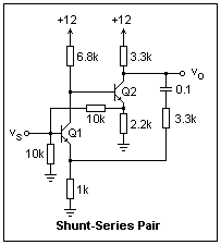 The circuit at the right has at least four feedback loops--can you identify them? Besides the two emitter resistors, there is a shunt-shunt feedback resistor whose upper end is fed by the emitter of the second transistor instead of by the collector of the same transistor. This follower supplies more current without causing a greater voltage drop in the collector resistor. There is an AC feedback loop (series-shunt) in which the 0.1μF capacitor blocks the DC bias. With this loop removed, the gain of the amplifier is about 12. The feedback factor is 1/4.3, so the loop gain is 2.8. Therefore, the gain with feedback will be about 12/3.8 = 3.16. I measured 3.11 on the circuit, at 1 kHz. This circuit is used for low-gain, wideband amplifiers, and is very stable. At high frequencies, large loop gains are dangerous. This example operates with a +12V supply, which rather restricts the "headroom" of the second transistor.
The Complementary Pair
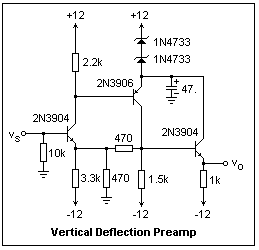 This circuit was suggested by a part of the vertical deflection preamplifier for a 100MHz scope. Quite a few resistor-capacitor combinations of a few ohms and a few picofarads have been eliminated, but the component values are the same as in the actual circuit. The eliminated components tweaked the response of the amplifier at high frequencies, otherwise having little effect. Note the two 1N4733 5.1V zener diodes to give +2V for the second two transistors. Of course, one 10V zener could be used, but this is what I had on hand. The circuit consists of a complementary pair of an npn and a pnp transistor. This use eliminates the need for coupling capacitors. The complementary pair drives an emitter follower to give a low output resistance (about 2.6Ω). There is strong series-shunt feedback between the two transistors, giving a rather small AC gain of 2.0. Note that most of the bias current of the npn transistor flows through the feedback network to ground, not through the emitter capacitor. The same thing happens in the collector of the other transistor. This is a case where the feedback network strongly loads the basic amplifier. There are many other similar circuits with more conventional feedback, if any.
Return to Electronics Index
Composed by J. B. Calvert
Created 16 July 2001
Last revised 18 July 2001