Microprocessor Experiments
Using a ROM emulator with an 8051 microcontroller
Contents
- The Romulator
- 8051 Notes
- A Basic 8051 System
- Using Interrupts
- References
The Romulator
Experimentation with microprocessors is an excellent way to become familiar with them, besides opening the possibility of creating small microprocessor-based control circuits. This is not really difficult, and experimental circuits can be built on solderless breadboards. Since we are not using printed-circuit boards, it is important to keep the amount of wiring within bounds, so 8-bit data buses and address buses no wider than 12 bits are very desirable.
General-purpose processors and microcontrollers are usually distinguished from each other, although they are very similar. A general-purpose processor has a single main address space to contain both program and data, and perhaps an additional I/O address space. A microcontroller may have separate program and data memory address spaces, the data memory often included in the processor chip, and often supports single bit I/O. Some modern microcontrollers, such as the PIC series, have EPROM memory on-chip. The 6502 and 8088 are two general-purpose processors that are easy to experiment with and make excellent microcontrollers. The 8051 and 6805 families are examples of microcontrollers. The 8051 has shown remarkable endurance, and is still actively in use. It is an extension of the 8048 microcontroller.
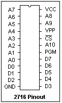 The prime requirement for experimenting with microprocessors is a source of program code. In a functioning controller system, this is generally in ROM (read-only memory) programmed beforehand. In the lab, programmable and erasable EPROM is frequently used. This requires a programmer and an ultraviolet erasing lamp, since an EPROM is generally reused over and over again. For experimentation, 2KB is quite sufficient. The classical EPROM of this size is the 2716, whose pinout is shown at the left. Because of the high programming voltage of the 2716 compared to later chips, many inexpensive programmers do not support it. The 2716 is also too small for most applications. One answer is to use 2732, 2764 or even larger EPROMS that are more readily available, but perhaps only use a 2KB portion by permanently tying certain address inputs to 0 or +5. The pinout of these standard EPROMS is similar, so that it can be arranged that any could be used in a circuit, as convenient. A 28-pin chip merely adds four pins at the top to accommodate additional address lines, supporting up to a 27256 with 32KB. CMOS EPROMS, such as the 27C32, use much less power than NMOS EPROMS.
For experimentation, a superior alternative is the ROM emulator (or perhaps "romulator", as it will be called here) that connects with the target system by a flexible cable and DIP plug that acts just like a 2716. Instead of a ROM, the romulator contains a read-and-write memory (RAM) chip like the 8418. This RAM is loaded somehow, and then the romulator takes the place of a ROM. The great benefit of this is that the contents of the RAM can be changed with ease, not requiring a UV lamp or a programmer for this purpose. The system controlling the romulator is called the "host" system, while the system under test is the "target" system. If you build the romulator yourself, it is also much cheaper than a programmer and UV lamp.
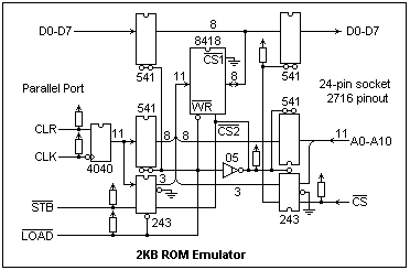 A 2KB romulator is shown at the right. Its core is an 8418 RAM chip, with programming circuitry on the left, and access circuitry on the right. The input to the programming circuitry is from the parallel port of the host computer. The parallel port supplies not only the 8 data values, but also 4 control bits that are used to operate the circuit. The 11 address bits are provided by the 74HC4040 counter. Note that 8 bits go through the 74LS541 buffers, 3 bits through the 74LS243. This counter can be cleared to 000 and then incremented by a strobe pulse. In this way, any address up to the maximum of 7FF can be established. When the address is established, the data is put on D0-D7 by the host computer, and then the /LOAD bit is pulled low, which enables the address and data buffers for programming. The /STB bit pulls /WR low, and writes the data in the 8418. This is repeated for each byte.
When /LOAD is high, the buffers on the left are disabled, and the access circuitry on the right is enabled. The 11 address lines are applied to the 8148, which then causes the corresponding data to appear on D0-D7. When the target system lowers /CS, the data output buffer is enabled, and the data appears on D0-D7, just as in the case of a 2716.
The main menu of the program written in C to support the romulator, ROME.EXE, presents the following choices: e, examine and modify buffer; d, dump buffer by pages to screen; f, fill with a given byte; t, enter ASCII text; b, search for a byte pattern; v, move bytes; s, save buffer to disk, l, load buffer from disk; p swap buffer and hold buffer; x, send buffer to romulator; h, program help; q, quit program. When the program starts, it determines which parallel port the romulator is connected to and reports it. The e command starts at any address, and displays the address and the byte currently there. A new byte can be typed in to replace it, or the byte can be retained. Pressing the space bar or entering a new byte goes to the next address. A note on screen warns when the romulator has not been updated after changing the buffer. Pressing Enter returns to the main menu. With the original version of this program, "x" should be excuted at startup to prevent later hangup. This bug will eventually be eliminated.
Other microcomputer development tools include the logic analyzer and the in-circuit emulator, both very expensive and much less helpful than they would seem. The logic analyzer is of little use with microcontrollers, since most of the circuits are not available for probing. The in-circuit emulator, or ICE, takes the place of the processor, and is essentially a software development tool. Its functions may be carried out in other, much cheaper, ways. The romulator is an equally powerful development tool. It may be combined with a debugging program that sets breakpoints and reports on status. For investigations regarding timing, a good oscilloscope is an excellent aid.
8051 Notes
The 8051 is a classic Intel microcontroller, in a 40-pin DIP. Of the 40 pins, 32 are devoted to four 8-bit I/O ports. There are VCC and VSS power pins, a reset pin RST, crystal oscillator pins XTAL1 and XTAL2, and /EA, ALE and /PSEN pins to support external memory access. A factory-programmed device has 4KB of program memory, and 256 bytes of internal RAM, divided into 128 bytes of data RAM and 128 bytes of special registers. 64KB of external program memory can be accessed when the /EA pin is grounded. The lower 8 bits of the address and the data are multiplexed on Port 0, the upper 8 bits are put on Port 2. The ALE signal is used to latch the low address byte, and the /PSEN signal is used to enable data applied to Port 0. 64KB of external data read and write memory is also supported, using Ports 0 and 2 as for program data, but also /WR and /RD strobes on Port 3, bits 6 and 7, respectively. Two timers and a serial transmitter and receiver are also provided, which can use other bits on Port 3.
A factory-programmed device has all four ports available for use. /EA (31) is tied to +5, ALE (30) and /PSEN (29) are not used. A crystal of up to 12 MHz is connected to XTAL1 (19) and XTAL2(18), each of these pins grounded through a 30 pF ceramic capacitor, and RST (9) connected to +5 through a 10 μF electrolytic capacitor. When power is applied, the system resets itself and begins execution at 0000.
The experimenter can use a factory-programmed device, if he ties /EA low and interfaces external program memory to Ports 0 and 2. This works for a factory-programmed device as well as for one that has no internal memory. Surplus factory-programmed devices are very cheap. A transparent latch, like a 74LS573, must be used with ALE to latch the address low. The 573 has a more rational pinout than the equivalent 273. The only other chip necessary is a ROM, usually an EPROM like the 2716, or the cable from the romulator can be plugged in like a ROM. The 8031 is an 8051 without the internal program memory, and must be used with an external ROM. It is very easy to get an 8031 running on a breadboard with a romulator.
The internal RAM acts like the registers in a general microprocessor, manipulated by short, efficient instructions. A direct address is a byte. An instruction may interpret the byte as a byte address affecting 8 bits at once, or as a bit address affecting only a single bit. The accumulator is merely the byte at address E0, but is also a built-in address for many instructions. The instruction MOV dest,src or 85 src dest, where src and dest are byte addresses, copies a byte from src into dest. The instruction MOV A,src or E5 src copies a byte from src to A, while MOV dest,A or F5 dest copies a byte from A to dest. Of course, the source of the data is not changed, although we often call the operation a "move".
It would have been intelligent for Intel to have implemented all the 256 bytes of internal RAM, and very easy to do, but stupidity won out and of the upper 128 bytes only those implemented as Special Function Registers are present. Otherwise, there would have been 102 more bytes available as a scratch pad.
For bits, the carry flag, which is bit 7 in the program status byte or PSW, acts as an accumulator. The bits that can be directly addressed are those in the 16 bytes 20 to 2F, and the 16 bytes 80, 88, 90, 98, A0, ..., F8. Bit addresses 00 to 7F refer to those in bytes 20-2F, while 80-87, 88-8F, 90-97, etc. are those in the bytes 80, etc., in the upper 128 bytes of RAM. The address of the carry bit is E7, since it is bit 7 in the byte E0. A bit is moved to C by MOV C,bit or A2 bit, and from C by MOV bit,C or 92 bit, where "bit" is a byte interpreted as a bit address.
One of eight things can be identified by three bits, say rrr. To construct short, byte-sized instructions for moving data, bytes can be identified in this way. The sets of eight bytes involved are called register bytes, identified as R0 to R7. There are four sets of eight bytes, called sets 00, 01, 10 and 11. Which set is to be used is determined by bits 3 and 4 in the PSW (bits E3 and E4). MOV A,Rn is the byte 11101rrr, E8 to EF, while MOV Rn,A is 11111rrr or F8 to FF. These single-byte instructions execute in one bus cycle. One can also use a direct address, as in MOV Rn,src or 10101rrr, A8 to AF and MOV dest,Rn or 10001rrr or 88 to 8F.
R0 and R1 are also used as pointer registers for indirect addressing. MOV A,@Ri is 1110011i, that is, E6 and E7. The byte in Ri is interpreted as a direct address, and the byte at that address is moved to A. Going the other way, MOV @Ri,A is 1111011i, F6 or F7. These are one-byte instructions. If a direct address is involved instead of A, we have MOV dest,@Ri or 1000011i, 86 or 87, and MOV @Ri,src or 1010011i, A6 or A7, followed by the direct address byte.
Immediate byte data is loaded into A by MOV A,#data or 74 data. It is moved into Rn by 01111rrr or 78-7F, followed by the data. It is moved to a direct address by MOV dest,#data or 75 dest data, and to an indirect address in Ri by MOV @Ri,data or 0111011i, 76 or 77, followed by the data.
All these instructions may seem complex, but they are constructed quite regularly. We have the locations A, Rn, direct or @Ri as sources or destinations, with immediate data as a further source. They are easily assembled by hand. Every byte except A5 represents a possible opcode. There is no instruction that halts the processor, which makes single-stepping difficult.
A few instructions load and store bytes from external memory. Since these are 64KB in size, two bytes are necessary to specify the address, and all addressing is indirect. The 16-bit address is stored in DPL and DPH at 82 and 83. These locations can be filled with immediate data by the instruction MOV DPTR,#data16 which is 90 followed by the high address byte, then the low address byte. That is, 90 02 F0 would load 02 in DPH and F0 in DPL.
External data memory is accessed by MOVX A,@DPTR, E0, or MOVX @DPTR,A, F0. Alternatively, MOVX A,@Ri or 1110001i, or MOVX @Ri,A or 1111001i, put only an 8-bit address specified by Ri on Port 0, leaving Port 2 unaffected. In either case, a single byte is moved from or to external data memory.
It is also possible to read data from program memory, in addition to the immediate data following instructions. In this case, A is used as an index register, and DPTR or PC as the base register. MOVC @A+DPTR is 93, while MOVC @A+PC is 83. Before PC is used, it is incremented to point to the instruction following the MOVC instruction. It is very convenient for a subroutine to be followed by tabular data in this way. One cannot write to program data.
One can add with or without carry, but one operand must be in A and the sum is left there. One can subtract with borrow (carry), again with the minuend in A and the difference left there. If there is no borrow, C must be cleared. There is a multiplication instruction (A4), with one factor in A and the other in B, the 16-bit product in B (high) and A (low). The OV flag is set if B is nonzero afterwards, and the C flag is cleared. The divide instruction (84) divides the dividend in A by the divisor in B, leaving the quotient in A and the remainder in B. OV and C are always cleared. B (byte 0F) is used only in MUL and DIV. These operations are on unsigned integers.
Any register can be incremented or decremented, specified by A, Rn, direct or @Ri. No flags are affected, so the registers roll over silently. The DPTR register pair can also be incremented, and DPH will be incremented when DPL rolls over. INC DPTR is C3. To facilitate programming loops, the decrement and jump if not zero instruction, DJNZ Rn,rel (D8-DF), or DJNZ dir,rel (D5 dir rel) is provided. Any byte can be used as a loop counter, and if an Rn byte is so used, the instruction is only a single byte. DEC A is 14, INC A is 04, both single bytes.
The short jump, SJMP, 80 rel can jump to a location 127 bytes ahead or 128 bytes behind the location following the instruction, since "rel" is interpreted as a signed byte. A long jump goes to any program memory location. The instruction is LJMP addr, 02 adh adl. The AJMP instruction specifies A0-A10 within the instruction, so it jumps anywhere in the 2K block in which the following instruction is located. It is rather unusual to have part of the address included in the opcode, but this saves a byte. There is also an indexed indirect jump, JMP @A+DPTR, which is only one byte, 73. The accumulator is added to the 16-bit quantity in DPTR, and a jump made to that address.
The ACALL instruction is like the AJMP, but the address of the instruction following the ACALL is pushed on the stack. This is two bytes, so that execution can return by a RET (22) instruction. The long call, LCALL, is 12 adh adl, calls any address in the 64KB code space.
An interrupt pushes only the two bytes of the PC, and disables interrupts of the priority level (and lower) of the interrupt being serviced. RETI (32) re-enables interrupts of this priority in addition to restoring the PC.
Only directly addressed bytes are PUSHed (C0 addr) and POPped (D0 addr), but this can include the accumulator (E0) and the PSW (D0). The stack pointer SP (81) points to the last byte pushed on the stack. PUSH increments SP and stores the byte at (SP). POP fetches the byte at (SP) and then decrements SP. The stack, therefore, grows upwards. On reset, SP is set to 07, so that the first byte pushed will be stored at 08. This is just above the first set of 8 register bytes, and may be satisfactory. If all four register sets are to be used, SP should be changed to 1F, or it the bit-addressable bytes reserved, to 2F. In the latter case, 80 bytes are available for the stack.
The conditional jumps are all short jumps using a signed byte relative offset that check the state of a flag bit. There is jump if carry set (i.e., C = 1), JC (40), and jump if carry not set (i.e., C ≠ 0), JNC (50). Any of the 256 addressable bits can be tested with JB (20), followed by the bit address and then the relative jump. JNB (30) jumps if the bit is not set. JBC (10) jumps if the bit is set, and also clears the bit. JZ (60) jumps if the accumulator contains 0, JNZ (70) if it does not. Each of these opcodes is followed by the relative jump, or by the bit address and the relative jump.
The accumulator can be cleared with a single byte, E4 or CLR A. This affects no flags, but the zero status of the accumulator can be tested with JZ or JNZ. The carry flag, the bit accumulator, can be cleared with the single byte C3, CLR C. Any bit can be cleared with CLR bit, C2, followed by the bit address byte. C can also be set with SETB C or D3. Any bit can be set with SETB bit, D2 followed by the bit address byte. The accumulator can be bitwise complemented, that is, 1 ↔ 0. Then, incrementing with 04, INC A, makes the 2's complement, which can be considered as the negative of the original number. Bits can be complemented as well, carry with CPL C, B3, and CPL bit, B2 followed by the bit address byte. A is the only byte register that can be complemented.
Two bytes can be compared, and a jump made if they are not equal. A can be compared with a direct byte using CJNE A,dir,rel, which is B5 dir rel, where dir is the direct address and rel is the relative displacement. The other compares are of A, Rn and @Ri with an immediate operand. All are three-byte instructions, an opcode followed by the immediate data and the relative jump. CJNE A,#data,rel is B4, CJNZ Rn,#data,rel is B8-BF, and CJNE @Ri,#data,rel is B6-B7.
The accumulator can be exchanged with Rn, @Ri, or a direct byte. XCH A,Rn is C8-CF, XCH A,@Ri is C6 or C7, and XCH A,dir is C5 followed by the direct address byte. SWAP A exchanges the high and low nybbles in the accumulator. Curiously, the low-order nybble of the accumulator can be exchanged with the low-order nybble of the byte whose address is in Ri with XCHD, D6-D7. The high-order nybbles are not affected. The exchanged nybbles usually represent BCD digits.
The accumulator can be rotated right or left through carry by RRC A (13) or RLC A (33). By clearing C before each instruction, logical shifts right or left can be done. By copying bit 7 of A to C before RRC, an arithmetic shift is done. An 8-bit shift can be done with RR A (03) or RL A (23), but these are less useful.
Bitwise logical operations are also carried out with the accumulator as one of the operands, except for operating on a direct byte with immediate data. ANL is AND, ORL is OR, and XRL is XOR. For example, ANL A,Rn is 58-5F, ANL A,direct is 55 dir, ANL A,#data is 54 data, ANL A,@Ri is 56-57, ANL dir,#data is 52 dir, and ANL dir,#data is 53 dir data. C can be ANDed with any bit by ANL C,bit or 82 bit, and with any bit complemented by ANL C,/bit or B0 bit. AND is often used to clear certain bits in a byte by ANDing them with 0 bits, but with the 8051 it is often easier to do this directly with addressable bits. There are similar instructions for ORL and XRL (XRL does not have bit instructions).
The ADD and ADDC instructions perform binary addition. If a byte is considered as containing two decimal digits ("packed BCD"), adding such bytes will not, in general, produce the correct decimal result. If we follow the addition with the DA A instruction, D4, the right numbers will be added, and the carries taken care of, so that the result is a correct decimal result. For example, if we add 76 and 55, we get the hex result CB. Adding 66, we have 131, which is a byte 31 and a decimal carry, which is the correct decimal result. Depending on conditions, 00, 06, 60 or 66 has to be added hexadecimally to get the correct BCD result. This only works for addition, and other tricks must be used in subtraction, multiplication and division.
A Basic 8051 System
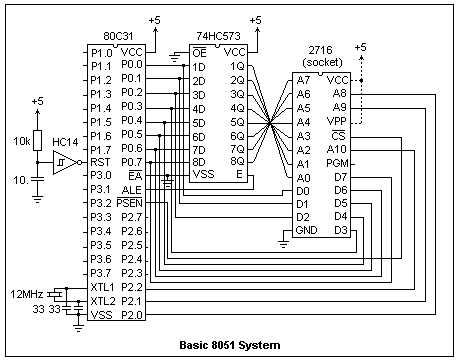 A basic 8051 system using a romless 80C31 is shown in the diagram. No I/O is shown, but LED's are easily added at Port 1 or Port 3, using the 74HC14 as a buffer (5 inverters are available). If the program comes from a romulator, the power connections shown dotted are not required. This is about the simplest computer system that can be constructed using external memory. Beside the microcontroller itself, there is only an address latch, and the inverter used to make the reset signal. This could, in fact, be replaced by a 10 μF capacitor to +5 (using an internal pulldown) and the inverter omitted. However, the inverters are useful as buffers, and this circuit gives a more reliable reset signal.
If external data memory is provided, the /WR strobe is at P3.6 and the /RD strobe is at P3.7. The latched A0-A7 is available, as is A8-A15 at Port 2. This circuit uses only A8-A10 for its 2KB of external program memory. Serial data is received at P3.0, and transmitted at P3.1. The active-low interrupts /INT0 and /INT1 are at P3.2 and P3.3. These should be driven by a flip-flop that can be cleared by the interrupt routine. The timer inputs T0 and T1 are at P3.4 and P3.5. Port 1, however, is not used for any special purpose and is always available.
The analogue of the "Hello, world!" program in high-level languages here in creating computer systems is making an LED blink at a predictable rate. This is a very simple accomplishment, but many things must go right for it to happen. It shows that your system can actually execute a program, which is its reason for existence. Once you can make an LED blink, you can go on to more meaningful problems immediately.
When the romulator is loaded, and the power is turned on to the target system, execution begins at 0000. If things do not work properly, which is very probable at first, it is not easy to find out what has gone wrong. The only evidence is provided by external observations. The ALE signal, at a frequency of 1/6 the oscillator frequency, is active if the system is running. The shortest loop is 80 FE; when the processor comes to these bytes, it will loop forever here, and at most only the lower two address lines will change. By looking at the address with a logic probe, it can be determined what point has been reached in the program. Instructions can be added to the program that output a diagnostic byte to a port. As the program proceeds, higher numbers can be output, for example. If there is a problem, the number showing at the port can tell how much progress was made. If Port 1 is used, for example, the instruction is 75 90 num, where num is the diagnostic number.
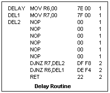 To blink an LED, we need a delay subroutine that just wastes time. A reasonable solution is a loop that counts down R7 from an initial value inside a loop that counts down R6. To decrement the counters, we can use DJNZ. A possible routine is shown at the left. A NOP (00) is a safe way to waste time. The 00 bytes give a maximum delay; they may be replaced by any values N6, N7 that give the desired delay. The inner loop requires 8 cycles, so the delay is (N7 x 8 + 3) x N6 + 2 cycles. The maximum delay is 525,058 cycles. A cycle is 12 oscillator periods, so with a 12MHz crystal each cycle is 1 μs. Therefore, for a 12MHz crystal, the maximum delay is about 0.5 s. This routine contains no absolute address references, so it can be placed anywhere that is convenient. Also, it does not use the accumulator or affect any flag.
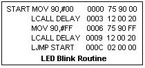 The main blinking routine is shown at the right. It assumes that the DELAY subroutine begins at 0020. Long calls and jumps are used for ease in modifying the program. ACALL and AJMP would be more economical in an actual program, saving one byte each. An LED connected to any bit of Port 1 will blink at about 1 Hz.
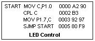 A routine for controlling an LED is shown at the left. The LED is driven by an inverter whose input is at P1.7 (bit 7 of Port 1). P1.0 can be connected either to +5 or GND by a wire. When this routine is run, the LED lights when P1.0 is connected to GND, and goes out when P1.0 floats. RESET writes a 1 to Port 1, which effectively prepares each bit for input by disconnecting the pin from active drive and allowing it to be pulled up by an internal pullup resistor. So that grounding P1.0 will light the LED, the input bit is complemented in C.
Using Interrupts
A microcomputer system can be requested to perform an action by an external signal, called an interrupt request. Since this request occurs at a time unrelated to program activity, it is said to be asynchronous. The 8051 has five ways to request an interrupt. Two are to place a low level on either pin 12, P3.2, or on pin 13, P3.3, which are called /INT0 and /INT1. The two internal timers can also interrupt the processor when they time out. The fifth source is the serial transmitter and receiver. We'll only talk about the external interrupts here.
Interrupts are not recognized unless they have been enabled. This is done by setting bits in the Interrupt Enable register at A8. Bit 0 enables the /INT0 input, while bit 1 enables the /INT1 input. For any interrupt at all to be recognized, bit 7 of this register must also be set. Therefore, to enable the /INT0 interrupt, bits 0 and 7, bit addresses A8 and AF, must be set to 1. Reset puts all zeros in IE, so interrupts are not enabled on power-up. The external interrupts may be requested by a transition from 1 to 0 on the pin, or by a low level on the pin. To enable a level interrupt, a 0 must be written to TCON.0 at 88. TCON.2 would do the same thing for /INT1.
When an interrupt is recognized, the processor waits until the currently executing instruction finishes, then disables interrupts and pushes the program counter on the stack, and passing execution to the interrupt vector at a particular location in program memory. For /INT0, this location is 0003, and for /INT1 it is 0013. The first three bytes in program memory are reserved for a jump to the beginning of the program after the processor has been reset. Location 0003 usually holds a jump to the beginning of the interrupt service routine.
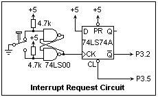 The interrupt must be requested in such a way that when the interrupt service routine returns, the request is not still active. Since the system responds so rapidly, this is not a trivial requirement. If you used an ordinary pushbutton, the processor could probably execute the interrupt a few hundred times before you could get your finger off the button. The circuit shown at the right, however, will do the job. The two gates of a 74LS00 serve as a debounced pushbutton which gives only one positive pulse on its output when the pushbutton is pressed. Without this, perhaps 5 to 10 pulses would be produced by the pushbutton when it is pressed and the contact bounces. This positive edge is applied to the clock input of the D-type flip-flop represented by the 74LS74A. This causes the level at the D input to be transferred to the output. In this case, the /Q output goes from 1 to 0. By the time the output changes, the input is again insensitive. The system clears the interrupt request by pulling the CL input low, which causes /Q to go back to 1. Each push of the pushbutton will cause one, and only one, interrupt request that is quickly cleared by the system. The P3.5 pin has been arbitrarily selected for the clearing, since we do not intend to use it for anything else.
If we had decided to use an edge interrupt request, it would be sufficient to use the debounced pushbutton alone, and the interrupt request would not have to be cleared by the service routine. In this case, TCON.0 would be set instead of cleared. TCON.2 does the same for /INT1.
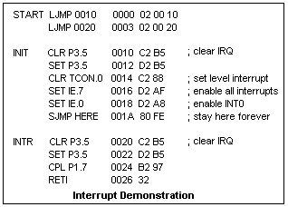 A program for demonstrating the /INT0 interrupt is shown at the left. An LED is assumed to be driven by an inverter whose input is at P1.7, and we wish the interrupt to toggle its state. After reset, the initialization routine is entered. The interrupt is cleared, in case it happened to be active, and then the IE and TCON registers are loaded with the desired values. After this, the main program has nothing to do but execute a short loop waiting for an interrupt. The interrupt service routine first clears the interrupt request, then reads the bit at the LED output, complements it, and puts it back in the output latch. This toggles the LED every time the interrupt executes, which should be every time the button is pressed. We do not have to re-enable interrupts before returning, as is necessary on many processors, because the RETI handles this for us. Bit 1 in TCON is a flag that is set when the interrupt is accepted, and automatically cleared by RETI. Often, an interrupt service routine must check to see what has caused the interrupt, but here the fact that the vector at 0003 was used shows that it is /INT0.
We have already seen that the vector for /INT0 is at 0003, and for /INT1 at 0013. For timer 0, it is at 000B and for timer 1 it is at 001B. The serial interrupt vector is at 002B. If a particular interrupt is never enabled, there is no need to keep these locations reserved. The service routine is short enough in the present case that it could begin at 0003 if we did not use the timer 0 interrupt. One LS00 and one LS74 is enough for two interrupt requests, so it would be easy to use both /INT0 and /INT1 to do different things.
There are two internal counters in the 8051. These count either machine cycles (a machine cycle is 12 oscillator periods), or negative edges on input pins. P3.4 is the input to counter 0 (T0), while P3.5 is the input to counter 1 (T1). Which source is counted and the mode of operation is specified by four bits in the TMOD register, 89. The upper nybble concerns counter 1, and the lower nybble counter 0. Bits 0 and 1 determine the mode. Mode 0 is an 8-bit counter with a 5-bit prescaler (13 bits in all). Mode 1 is a 16-bit counter. Mode 2 is an 8-bit counter with automatic reload when it goes from FF to 00. Mode 3 uses counter 0 as two 8-bit counters, one controlled by the usual counter 0 control bits, the other by the counter 1 control bits. Counter 1 is stopped in this mode. If bit 2 is set, input is from the system clock, while if it is clear, input is from the T0 or T1 line. Bit 3 is the gate bit. When it is 0, the counter is started and stopped by the state of bit TR0 or TR1 in TCON. To put counter 0 in mode 2, load 02 into TMOD. To put both counters in mode 2, load 22.
Each counter has two counter bytes, TL0 (8A) and TH0 (8C), TL1 (8B) and TH1 (8D). In mode 0, TL counts and TH prescales. This mode is provided for compatibility with the earlier 8048 microcontroller. In mode 1, both TH and TL are used. In mode 2, TL is the counter, and TH holds the reload byte. In mode 3, TL is the usual counter 0, while TH is the other counter. This, in effect, adds another counter. These locations should be properly loaded before the counters are started. All the counters count up.
When a counter rolls over from FF to 00, an interrupt may be requested. This is really the only way to use the counters for general purposes. The flags that request the interrupt are TCON.5 or TF0 for counter 0, and TCON.7 or TF1 for counter 1. The system generally handles these flags, and the programmer need not test them. They are set by the counters, and cleared by RETI. TCON.4 or TR0 turns counter 0 on and off as it is set or clear. TCON.6 or TR1 does the same for counter 1. The programmer must set these bits to start the counters. Their bit addresses are 8C and 8F, respectively.
The interrupts are enabled by setting bit 1 (A9) for counter 0, or bit 3 (AB) for counter 1, in the IE register. Bit 7, EA, must also be set to enable interrupts. The vector for counter 0 is at 0003, and 000B for counter 1. To use a counter, then, it must be initialized to the desired mode (TMOD), loaded with a starting value (TH and TL), the interrupt enabled (IE), and the counter started (TCON).
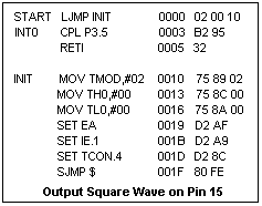 Let's output a square wave at P3.5. A program to do that is shown at the right. The interrupt service routine is only three bytes long, so it can be placed at the vector location. This gives the lowest possible frequency of the output square wave. With a 6 MHz oscillator, this frequency is about 1 kHz. The maximum frequency is about 125 kHz, with FF loaded instead of 00. There is a minimum period of about 4 cycles.
Interrupts are particularly useful for embedded systems, perhaps to initiate periodic actions such as reporting conditions, or for taking actions when a particular external event occurs. An interrupt is recognized within a few microseconds, so it can handle rapid events. The 8051's vectored interrupts facilitiate a rapid response. If more than two external interrupts are required, the requests may be ORed on an interrupt request pin. The service routine must then poll the possible sources to determine which source is active. Another way to monitor external events is to test an input bit with JB or JNB.
References
__________, 8-Bit Embedded Controllers (Mt. Prospect, IL: Intel, 1990).
Return to Math Index
Composed by J. B. Calvert
Created 30 September 2004
Last revised