A function that is often useful is conversion from a voltage to a frequency (which is a wide-range voltage-controlled oscillator) or from a frequency to a voltage. This may be useful in telemetry, where a frequency can get through a link, such as a telephone line, while a direct current cannot. Another application is tachometry, where a voltage proportional to speed is desired, and an alternating voltage can easily be generated proportional to speed. It is also fun, and a good illustration of some of the circuits in other units of this series.
Since these functions are so useful, it is no surprise that integrated circuits have been created where everything needed, except for some resistors and capacitors to set the parameters and act as filters, is in one package. We will use such packages here. For voltage to frequency conversion, the LM331 is available in an 8-pin DIP, looking much like an op-amp. Going the other way, we will use the LM2907, which comes in a 14-pin DIP. Incidentally, the LM prefix refers specifically to National Semiconductor, but there are other sources, and these will use their own prefixes. The prefixes are so that government orders using them will also choose the manufacturer at the same time, under the supposition that a different prefix is a different part. Also, there are often similar parts with slightly different specifications, usually in the operating temperature range. The 331 is specified from 0°C to 70°C, the "commercial" range, while the 231 and 131 have extended temperature ranges (which are of no benefit to most users).
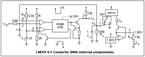
Let's start by building a voltage to frequency converter. The insides of the 331 from an operational viewpoint are shown in the figure below. The pins numbers are marked beside the circles representing them. All the external components are shown that are necessary to make a working circuit. The diagram is a little complicated, so it will be explained piece by piece. All the stuff around the box marked "single shot" is for the purpose of holding the voltage at pin 1 (on the right) the same as the input voltage Vin (on the left). The 100k resistor and 0.1 μF capacitor are a low-pass filter to eliminate rubbish in the input voltage, and can be neglected in what follows. The input voltage and the voltage at pin 1 are fed to the inputs of a comparator, the triangle. When the voltage at pin 1 drops below the input voltage (comparing the voltages at pins 6 and 7), this comparator triggers the single shot, which then fires, saturating the output transistor and pulling pin 3 to ground.
This turns off the transistor that was holding the timing capacitor Ct to ground, and allows its voltage to rise, pulled up by timing resistor Rt. We have a relaxation circuit here. When the capacitor voltage reaches 2V/3 (given by the divider of internal resistances R and 2R), the single shot times out, after a time t = 1.1RtCt. The output transistor is released, and the output goes high again, pulled up by the external 10k to any desired logic voltage, not necessarily the supply voltage to the package. We now have to explain how the voltage at pin 1 is pulled up above Vin by all this. This is accomplished by putting a slug of charge on the output capacitor CL. This comes from the current mirror, which supplies a current Is when the switch SW, controlled by the single-shot, is in the position shown. The slug of charge is Q = Ist, where t is the time that the single-shot is on. This raises the output voltage by Q/CL, which usually does the job. If it does not, for some reason, the single-shot will fire again, and keep doing it as long as the voltage at pin 1 is less than the voltage at pin 7.
All the time, however, CL is discharging through RL, so the voltage always drops and kicks off the single-shot again and again at a rate that depends on the voltage, since the average current to the load capacitor does not change. By a current balance, then, we have Istf = V/RL, or f = V / (IstRL). The output frequency is directly proportional to the input voltage, which is precisely what we want. By choosing good capacitors and resistors, the proportionality can be made very constant, and high accuracy can be obtained.
Is is determined by the components on the extreme right of the diagram. There is an accurate, internal band-gap source of 1.90 V that is buffered by the op-amp, and supplied to pin 2. Any current leaving this pin is sent to the current mirror, and is accurately copied as Is. Therefore, in this case, Is = 1.90 V / 15k = 127 μA. For the values shown in the diagram, we should have fo = 1055V Hz. When I tried the circuit, using voltages from 0.1 V to 9.91 V, I found ratios of frequency to voltage from 1078 to 1159, measuring the frequency roughly with the oscilloscope. Had I used a proper frequency counter, the results would have been more consistent.
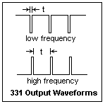 Output waveforms are shown at the right. Note that the low times are all the same length, t, which in this case should be 75 μs, which was exactly what I measured with the scope. Note that t limits the highest frequency that can be obtained. Results for this circuit are satisfactory from about 100 Hz to about 10 kHz, for input voltages from 0.1 V to 10 V. The values can be trimmed to get an even factor, say of 1000, so that a frequency counter will display voltage directly (if the decimal point is moved appropriately).
The 331 can also be used as a frequency to voltage converter. The idea is to trigger the single-shot at the rate of the input frequency, and look at the voltage that results at pin 1. This usually requires that the input be differentiated with an RC circuit to get trigger pulses. This would be easy enough to do, but instead we shall use an IC that is made specifically for this purpose, the 2907. The internal works, and the external components necessary to make a functional circuit, are shown below.
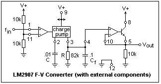
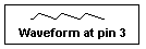
This is a good deal simpler than the 331, and consists of two separate modules. On the left is the frequency-to-voltage converter proper, and on the right is an op-amp driving a transistor, used for buffering the output voltage from the converter. There is a differential input, and the comparator detects crossings of the inputs, and triggers the current pump for each one. In this case, the inverting input is tied to a voltage divider furnishing V/2 as the reference voltage. Every time the input to the noninverting input crosses this value, the charge pump will pump. What it does is pump a charge CV/2 into and out of the capacitor C, and furnishes an equal charge, always in the same direction, to the resistor R. The voltage drop across the resistor is the output voltage. Capacitor Cf is a filter capacitor, to smooth out the voltage at pin 3, which otherwise would consist of spikes. The resulting waveform at pin 3 is sketched below.
 The op-amp simply buffers the voltage at pin 3, driving the base of a transistor whose emitter and collector are both available, so just about anything you want can be done with the output. Note the feedback loop to the inverting input. You can connect the output of the 331 directly to pin 1 of the 2907, to create a voltage-frequency-voltage converter. The manufacturer says that the output voltage V = finVCCRC, but I did not get this value when I tried the circuit. What I found was V/f = 0.0023 V-s, while the value calculated from the formula, with measured component values, was 0.0099. I have not taken the time to investigate the discrepancy, and leave it as an exercise for the student (for now). The circuits, however, worked very well, the ratio of the input to the 331 to the output of the 2907 varying very little from a constant 2.54.
The 2907 also comes in an 8-pin DIP, called the 2907N-8, and has some internal connections. The inverting input of the crossing detector is connected to ground, so that it detects zero crossings. The input is protected so that it can swing above and below ground, all will be right so long as it the input voltage does not exceed 28 V. Also, the output op-amp is permanently connected to buffer the output voltage. In this version, the input is pin 1, the capacitor is connected to pin 2 and the resistor to pin 3. The transistor emitter is pin 4, and its collector is pin 5. Pin 6 is V+, pin 7 the inverting input of the buffer op-amp, and pin 8 is ground (!). When using the 2907, be careful not to pull either of the inputs below ground unless there is a series resistance in the circuit to limit the current to the substrate. It is usually bad news to take any pin beyond the supply rails in any kind of chip. The 2907N-8 is, apparently, designed to skirt this rule. There is also a 2917, which has an internal 7.56 V Zener diode regulating VCC for the chip. This is intended for automotive applications where the supply voltage is notoriously variable.
Composed by J. B. Calvert
Created 22 July 2001
Last revised