Looking at the 4046, 567 and 565 PLL's
The phase-locked loop (PLL) is a device with many interesting applications, including frequency synthesis, FM demodulation, and television sweep circuits. Its operation seems nearly miraculous, but feedback makes the job easy, and it is an excellent example of feedback in action. Phase-locked loops, despite their importance and interest, are usually not treated in a university electronics course, though they are very much electronics and help the understanding greatly.
We will consider the fundamental phase-locked loop here. Once its operation is understood, all the applications will follow easily. We generally think of the circuit as accepting an input at some frequency and providing an output at the same frequency that is not a copy of the input, but the output of an independent oscillator whose frequency is controlled by feedback. The output of the oscillator is compared to the input, and if the frequencies are different, the frequency of the oscillator is altered to reduce the difference.
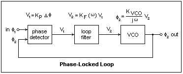
This is what it looks like, but it is better to consider the controlled quantity to be the phase of the signals. A signal of frequency f Hz changes phase by 2πf radians per second. In general, the phase in radians is 2π times the integral of the frequency with respect to time. The phase-locked loop compares the phases of the input signal and the oscillator signal, and adjusts the oscillator to reduce the phase difference. A signal flow diagram of a phase-locked loop is shown below.

The left-hand block is the phase detector, which compares the phases of its two input waves and provides an output V1 proportional to the phase difference Δφ. KP is a constant with the units volts per radian. The output of the phase detector is usually in the form of pulses that have to be low-pass filtered by the loop filter, the middle block. In the frequency domain, the loop filter is characterized by some function KF(ω), which multiplies the frequency domain representation of V1, V1(ω) to provide the control voltage V2(ω). This signal is then applied to the voltage-controlled oscillator or VCO, the block on the right. The division by jω is the frequency domain equivalent of integration in the time domain, as we know, and turns the frequency output into phase output. The polarities must be arranged so that if φ2 lags φ1, the VCO increases frequency slightly; that is, the feedback must be negative. The output of the VCO is fed back to the phase detector, and the feedback loop is closed.
The most important part of the feedback loop for the designer is the loop filter. It is basically a low-pass filter with a corner frequency that should be well below the signal frequencies, so that the control voltage to the VCO is relatively steady. However, the PLL must be able to respond to changes, so the corner frequency should be above the frequency of those changes. Quite often, we want a PLL that responds rather slowly, to provide a flywheel action that damps out noise and unwanted variations. It is a delicate matter of compromise, and the designer's tool is the loop filter.
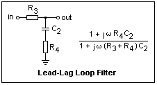 The simplest really satisfactory loop filter is the so-called lead-lag filter shown at the right. It is just an RC low-pass filter with an extra resistance in series with the capacitor. At low frequencies, its gain is 1, while at high frequencies it is a resistive divider with gain R4 / (R3 + R4). The frequency response function is said to have a pole at 2πfc = 1/(R3 + R4)C2 and a zero at 2πf2 = 1/R4C2. The pole provides a phase lead, while the zero a phase lag, so that the phase is zero both at low and high frequencies. It is easy to draw a Bode plot of the phase variation, as well as of the gain. One method of loop filter design is to determine satisfactory values for fc and f2, and then to proportion the filter reasonably. The resistors can be larger if the capacitor is smaller, and vice-versa. The values depend largely on the input resistance to the VCO; if this is high, anything goes, just about.
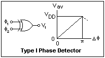 Let's take a brief look at phase detectors. The simplest type, and a good one, is shown at the left. Detectors of this kind are called Type I. It is simply an exclusive-or (XOR) gate that gives a high output when the signals are of opposite sign, and a low output when they are of the same sign. When the signals are in phase, the output is 0, while if they are in antiphase, or with phase difference π radians, the output is a constant high value. If the two signals are of different frequency, the phase relation will change continuously, and the output will be a series of pulses. The effect on the VCO will be to change the frequency first one way, then the other, but in general the changes in the proper direction will be a bit longer, and will win out in the end, raising the VCO frequency to the input frequency. Then the phase relations are stable, and the delay is just enough to provide the average voltage necessary to the VCO. The two signals are brought to the same frequency, but not necessarily to the same phase. Nevertheless, the phase difference is constant.
A second type of phase detector, Type II, is a much more complicated sequential logic machine that compares the delay between edges of the input signal and the VCO output. If the input signal leads in phase, positive pulses are produced with a width equal to the difference. If the input signal lags in phase, the pulses are negative instead of positive. The pulses are integrated on the filter capacitor, and the average value controls the VCO. In this case, the phases will be brought into coincidence, not simply to a fixed difference. The oscillator wave will be exactly locked to the input wave. Pin 1 outputs the phase pulses themselves, while pin 13 is the normal output to the loop filter.
The process of capture is the transient state in which the VCO control voltage is trying to acquire a value that will make the phase relations stable, as when the circuit is first turned on, or the input signal first applied. This can only be successful when the control range of the VCO includes the input frequency. Otherwise, the loop will never lock. If the control range is proper, then with a Type II detector lock will always eventually occur. With a Type I detector, if the signal and VCO free-running frequencies are too far apart, the filtered output of the detector will not be sufficient to raise the VCO control voltage the required amount, and there will be no capture. This behavior is useful in detecting signals of certain frequencies. Once a loop is locked, it will follow the input through the whole range of the VCO, which may be larger than the capture range.
One more thing must be considered in loop filter design. In any feedback circuit, the possibility of instability and oscillation is a very real threat, and must always be taken into consideration. Phase-locked loops are not exempt from this warning. The loop filter must be designed to ensure stability. Instability occurs if the loop gain A approaches an absolute value of 1 with a phase shift of 180°. Then, 1 + A = 0 and we have oscillation. Instability is prevented if the phase shift when the absolute value of A drops to unity is guaranteed less than 180°. We know that the phase shift of a single-pole response is 90°, so if we force the output to have a single-pole falloff, then we have a leeway of 90° before bad things happen. This is usually ample, and allows for some added phase changes that we have not taken into consideration. This situation is exactly the same as for op-amps.
The loop gain A is the product of all the gain factors around the loop. The VCO integration to get phase introduces a pole, and a simple RC filter (R4 = 0) would introduce a second one. The result guarantees a phase shift of -1 at some high frequency, and oscillation. Actually, in some cases such a simple filter may work if it has a very long time constant, but usually will not if a nimble PLL is desired. The zero introduced by the lead-lag filter is just what we need. All we have to do is to ensure that f2, the corner frequency of the zero, is lower than the frequency f1 at which the absolute value of the gain becomes 1. To find f1, you can assume that the loop filter is operating like a resistive voltage divider at this frequency, leaving only the 1/jω from the VCO. This frequency cannot be chosen at random, but is determined by the feedback network you use, so there may be a little iteration necessary in finding it. If f2 < f1/5, everything should be all right.
There is a wonderful integrated circuit that contains all the parts necessary to make a PLL except for a handful of resistors and capacitors, the 4046. It was originally a standard CMOS product with a wide supply voltage range (to 15V). Now it is also available a an HC part, the HC4046, with maximum supply voltage of +7 V. You can use either one for the experiments of this section. The 4046 is designed to be used with square waves, which actually makes it easy to study on the breadboard. For the full glory of these investigations, you will need an oscilloscope, a function generator and a frequency counter in addition to your DMM. Nevertheless, it is all worth it. The circuit is shown below, together with the contents of the 4046 and its pinout. Not shown is a 7 V Zener diode whose anode is connected to pin 15, and whose cathode is connected to pin 8, to be used for power supply regulation, in the case of the CMOS 4046.
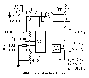
The two separate parts of the 4046 are the phase detectors, one Type I and one Type II, and the VCO. The voltage input to the VCO is at pin 9, and its square-wave output is at pin 4. A follower is provided for measuring the VCO control voltage at pin 10 without loading anything. This voltage is sometimes the desired output. C1, R1 and R2 control the frequency range of the VCO. The graphs given in the data sheets for the selection of values were highly unsatisfactory and difficult to read; in addition, they did not seem to correspond to reality. Both resistor values affect the center frequency of the VCO (at control voltage VDD/2). A large R2 corresponds to a wider frequency range. For R2 infinite (i.e., absent) the frequency starts near zero for zero control voltage. The values shown gave a range of approximately 11 kHz to 22 kHz.
The first procedure is to connect +5 and ground, R1, R2 and C1. Pin 5, "inhibit," should be grounded. If brought to VDD, it shuts everything down and reduces the current drain from the power supply. Also ground input pins 14 and 3. CMOS inputs must not be allowed to float when they are not in use, as can be done with TTL logic. Now, vary the voltage applied to pin 9 with a potentiometer over the range 0 to +5 V, and measure the output frequency at several values. The VCO gain, KVCO in radians/sec/volt can now be found (multiply by 2π to go from Hz to radians). I got 1.357 x 10⁴ rad/s/V.
If we use phase detector II, the gain KP = 5 V / 2π radians = 0.796 V/rad. For phase detector I, the phase range is π, so the gain is 1.592 V/rad.
We do not have the loop filter designed yet, but as a rule of thumb is it satisfactory to make R3 = 5R4, which is a good starting point. This makes the high-frequency gain of the lead-lag network 1/6 = 0.1667. Putting this all together, we find a loop gain of 1947/jω. The absolute value of this goes to unity at f1= 310 Hz. If f2 is made a fifth of this, or 62 Hz, we will have the desired behavior and sufficient phase margin at f1 to prevent instability. The low-pass corner frequency is chosen to be fc = 10 Hz, which will allow the PLL to follow at about this speed, which should handle any manual variations in input frequency. These values give, selecting an 0.1 μF capacitor, R3 = 130k and R4 = 27k.
Now connect the loop filter, and join pins 3 and 4 to complete the loop. Couple the function generator (set for square waves, and with output level all the way down) to pin 14 with an 0.1 μF capacitor. Use one channel, say Ch 1, of the scope to look at the input signal at pin 14, and Ch 2 to look at the output of the VCO, at pin 4. Trigger the scan on Ch 1. Read the VCO DC control voltage at pin 10 with the DMM. Turn on the power, and then the function generator. Bring the input voltage up to about 4 V amplitude. When you adjust the input frequency until it is within the VCO range, you will see that Ch 2 is no longer random, but there is an exact copy of what is on Ch 1, in exactly the same phase. Adjust the input voltage until it is equal to the VCO output voltage. When you move the input frequency outside the VCO range, lock will suddenly be lost and Ch 2 will go random. Vary the input frequency over the VCO range, noting the corresponding VCO control voltages. They should be the same that you measured when finding the gain of the VCO. The PLL is a frequency-to-voltage converter of a different type than we have met before.
Try a very conservative loop filter with R3 = 1M and R4 = 220k. This filter has fc = 1.3 Hz, and gives a very stable loop. Now change from phase detector II to phase detector I. You will have to get close to the free-running frequency to capture, but then it will lock over the full range. Notice the phase relation between Ch 1 and Ch 2 as the frequency is varied; it is not zero, and must increase to raise the VCO control voltage. This kind of phase detector works best for noisy input signals, since it does not depend on recognizing edges, but integrates over the waveforms.
A useful device that uses a PLL is the 567 tone detector. Here you do not get to fiddle with the loop as much as with the 4046, but this makes the circuit easy to use. The center frequency of the VCO is set by a timing resistor Rt and timing capacitor Ct: fo = 1/1.1RtCt. This relation does appear to be obeyed, more or less. The maximum oscillator frequency is at least 100 kHz, but 500 kHz is typical. The power supply at pin 4 (!) is 10 V maximum, but the open-collector output at pin 8 can be pulled up to 15 V if desired. The input at pin 3 can be pulled from 10 volts below ground to 0.5 V above pin 8, but should be capacitor coupled to avoid any unwanted currents. The input resistance is about 20k.
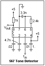 A typical circuit using the 567 is shown at right. The values shown provided fo = 150 kHz, although the formula gave 115 kHz. The capture bandwidth depends on the input voltage and oscillator frequency, and also on the loop filter capacitor connected to pin 2 (here 4.7 nF). The bandwidth can be estimated from the formula BW = 1070 sqrt(Vi/foClf) in % of fo. Clf is in μF, Vi in V, and fo in Hz. The maximum bandwidth is about 14%. The formula for this circuit gave 14%, about the maximum. The capacitor on pin 1 filters the output at pin 8, while the capacitor at pin 4 decouples the power supply. These values were the ones furnished in the application notes for the device, but any reasonable values can be used. Only the timing capacitor and the loop filter capacitor affect the operation of the PLL. This circuit was found to lock from about 139 kHz to 159 KHz, which agrees with the bandwidth formula.
The output is taken from the open collector at pin 8, filtered by the capacitor on pin 1. This pin will sink 100 mA, so a considerable load can be switched. The rise and fall times are advertised at 30 ns and 150 ns, respectively, for a typical device.
 A circuit that produces two outputs in quadrature, 90° apart in phase, is shown at the left. The output at pin 5 should probably be buffered, but the application notes indicate that it can handle a load of anything greater than 1k input resistance. The power and ground connections are not shown in the diagram, and are the same as in the basic circuit.
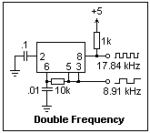 The circuit at the right produces two outputs, one at twice the frequency of the other. If pin 5 is connected to pin 1 instead of pin 3 (this merely passes the oscillator output to the output transistor), the same waveform appears on pins 5 and 8.
 The 565 is a bipolar chip that, like the 4046, contains a phase detector and a VCO. These modules are not completely separate, as they are in the 4046, so they are a little more difficult to experiment with individually. The input to the 565 is intended to be a sine wave, or something similar, so the phase detector is designed accordingly. It is a double-balanced modulator, and does for analog signals essentially what the XOR gate does for square waves. It is a Type I phase detector, with a range of 0 to 180° in phase. The circuit is shown at the left. The inputs at pins 2 and 3 of the 565 are directly to the bases of the input transistors. The square wave from the VCO switches the transistors that are conducting at any moment, and the outputs are taken differentially from the collectors. There is a minimum output for zero phase difference, and a maximum for antiphase. The output is sent through amplifying circuits directly to the VCO, whose DC input appears at pin 7. This is from 8 to 10 V, so a reference voltage is output at pin 6 to make connection with op-amps easier.
The loop filter is connected between pin 7 and VCC (not ground). At its simplest, it is simply a capacitor of fairly large capacitance. A lead-lag filter can be made by connecting a resistance in series with this capacitor, also adding a smaller capacitor directly from pin 7 to +V. There is an internal 3.6k resistance in series with pin 7 that provides R3. The 565 can be used at supply voltages up to ±12 V, and will function up to 100 kHz or so. In the experiment, we use ±12 V, because that is what we have, but the data sheets suggest that ± 6 V is more typical. The center frequency is set by Rt and Ct, and will be not far from fo = 1 / 3.7RtCt. The formula is correct, but the graph in the data sheet was incorrect (this was an old data book; there may be a correction). The values used in the experiment below gave 27.88 kHz, while the calculated value was 27.03 kHz.
 A circuit for studying the 565 is shown at the right. Note that both inputs are returned to ground through 470Ω resistors, so there is no trouble with bias currents to the bases, and the input from the function or signal generator is through a coupling capacitor. Set the signal source for a sine wave output, and an amplitude of about 2 V peak-to-peak. It must be at least 1 V p-p for the PLL to work. Connect scope leads as shown, Ch 1 at the input, and Ch 2 at the VCO output. Connect a frequency counter to the input, and measure the VCO control voltage with the DMM at pin 7. Don't try to measure the VCO gain as we did for the 4046--pin 7 has a limited range of voltages for which the circuit will function, and we will make this measurement another way. Turn the power on, then the counter and the signal source. Vary the frequency until the PLL locks, which will happen around 25-30 kHz. Observe that the following range is greater than the capture range. To narrow the capture range, connect a resistance between pins 6 and 7. Leaving this open, as we have, makes the capture range as large as possible. Shorting it makes the range as small as possible. Measure the VCO control voltage at pin 7 while varying the frequency. I found from 7.99 V at 35.5 kHz to 9.87 V at 20.2 kHz, which was about the maximum lock-in range in this case. As you vary the frequency, note the phase relation between the input and the VCO output, which changes as expected for a Type I phase detector.
Although we can find KP and KVCO well enough, there are internal mysteries in the rest of the loop that make estimating the loop gain as a function of frequency more difficult than with the 4046. The data sheets give some help in this exercise, plotting the loop gain as a function of the resistance between pins 6 and 7. Further experimentation could reveal some details, but it is not worth it here. A simple capacitor loop filter appears to work in this case, but will not be optimum in critical applications. The 565 works better than the 4046 for sine wave inputs, because of the more appropriate phase detector.
Composed by J. B. Calvert
Created 24 July 2001
Last revised 10 September 2007