Transisting
How transistors work, and how you can make switches and amplifiers with them; the LM386 integrated circuit amplifier
The Search For An Amplifier
From the very beginning of electronics, there was a search for some means of making one circuit control another electrically, especially so that a weak signal could be made strong. The first device to do this was the electromagnetic relay, a device still in widespread use. The coherer of early radio was essentially a relay, in which weak rf currents would cause a powder to cohere and become conducting. Both these devices are on-off, binary devices, but a proportional control would permit much wider applications, in telephony, audio and other fields, as well as in radio. The input or control should require very little power, while the output should control large powers, and the output should reproduce the input as closely as possible in form. The basic idea of an amplifier is power gain--more signal power out than in, the additional power coming from some external source.
The triode vacuum tube met these requirements very well. It was technical heroism to use a stream of electrons in a vacuum for this purpose, something that scarcely seemed practical. Nevertheless, vacuum tubes were produced in great variety and number, with both glass and metal envelopes, that had reasonably long lifetimes and were economical enough to find their way into consumer electronics. The electron stream was controlled by the electric field of a grid electrode that was largely ignored by the strong electron stream that passed from cathode to anode. The grid simply opposed the attraction of the anode in the critical region near the cathode that controlled the current, and drew very little current itself. In this way, large currents were controlled by a voltage applied between grid and cathode.
All during the time of the vacuum tube, efforts were made to create a device using the electrons that moved in solids, so that the expensive and troublesome vacuum, as well as the expense of heating the cathode and the necessary high voltages, would not be required. This was impossible in a metal, but perhaps semiconductors could be used. Every attempt to do this failed until the late 1940's, when a solid state amplifying device was finally created, although it operated on a very different principle from the one that was expected to work. When the methods of fabricating semiconductors were better developed, the original idea was realized in the field-effect transistor, which in many forms is now widely used. However, the junction transistor, which is the subject of this page, has been extensively developed and is a very useful tool in electronics. It takes over from the vacuum tube in the same applications, with all the desirable characteristics of low cost, reliability, small size, and lack of a vacuum, that were sought.
How A Transistor Works
The junction transistor consists of two PN junctions in the same crystal that are very close together. In the npn transistor, there is a region of n-type semiconductor (negative electrons the majority carrier of current) from the more positive electrode, called the collector, to the more negative electrode, called the emitter, through which the main (output) current passes. The collector and emitter regions are separated by a thin p-type region (positive holes are the majority carrier of current) called the base. Whatever way you try to pass current from collector to emitter, this p-type base region prevents it, just as in the familiar rectifying diode. The PN junction between the collector and base does the job when you try to pass current from collector to emitter, the usual direction for the npn transistor. The other PN junction, the one between base and emitter, is in the proper arrangement to pass current in this direction. If you make the base positive enough with respect to the emitter (about 0.7 V), this junction will begin to pass current in quite a large amount. However, the electrons injected from the emitter never reach the base contact. Instead, they fall into the collector junction. Normally, there are very few electrons in the base, and so the collector current is small. When you forward-bias the emitter junction, however, there suddenly are lots of electrons and the current flows to the collector instead of the base, as it would do if the two junctions were any distance apart.
It should be clear now how a transistor works. Just as in a vacuum tube, the input voltage causes a large current to flow, which is not intercepted by the grid (in the vacuum tube) and passes on to the anode. In the transistor, this current is created in the emitter junction, and then passes right by the base. In either case, a small voltage controls a large current.
The current I through a PN junction due to a forward bias voltage V is given rather well by the formula I = IS[exp(V/nVT) - 1], or, for all practical purposes, simply I = ISexp(V/nVT). The quantity VT, the thermal voltage is kT/e, where k is Boltzmann's constant, T the absolute temperature, and e the magnitude of the electronic charge. At room temperature, VT is about 25 mV. For most transistors under normal currents, n = 1. It is remarkable that this simple relation applies to all junction transistors. As a first approximation, if V is the voltage between base and emitter, then I is the collector current.
As you probably know, some base current does flow, and the amount is proportional to the collector current. In fact, IB = IC/β. The quantity β is called, well, beta, and depends mainly on the collector current. It is very difficult to control the value of beta in manufacture, so different transistors of the same type may have rather widely different values of beta. Any good transistor circuit is arranged so that the value of beta has very little effect, so long as it is in the range expected for the transistor type chosen.
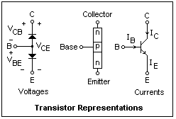 Three representations of an npn transistor are shown in the figure. In each, the collector, base and emitter terminals are identified. At the left is a representation as two diodes, or PN junctions, which only serves to show how the interelectrode voltages are designated. The order of the subscripts shows the plus and minus sides. At the right is the usual circuit symbol. Note the arrowhead that identifies the emitter lead and the type of transistor. It is in the direction of normal current flow; in this case, it shows that the transistor is an npn type. The usual positive directions of the terminal currents are shown here. In the middle is a representation as a bar of semiconductor crystal, with the thin base layer between the collector and base regions. Actual transistors do not look like this inside, but the idea is the same.
A pnp transistor operates the same way, except that the normal currents and polarities are reversed. In the circuit symbol, the emitter arrowhead points toward the base. Since most circuit diagrams are drawn so that currents flow from top to bottom, and signals from left to right, the emitter is usually placed at the top of the symbol, and the collector at the bottom. Since pnp transistors depend on the flow of holes, which is not as easy as that of electrons in silicon, their characteristics are a little inferior to those of npn transistors. Still, to a first approximation, npn and pnp transistors can be considered mirror images, something that did not exist with vacuum tubes.
Transistor Ratings
 There are many different transistor types, but all act similarly in a circuit. As examples, we will take the 2N4401, 2N4124 and 2N3904. These are three small-signal npn general amplifiers and switches, all appearing in the familiar TO-92 package with three leads. The connections are shown in the figure. On the left-hand side, you are looking at the transistor from the end the leads protrude from; on the right-hand side, the flat face is facing you. Not all transistors use these connections, though many do. Before using an unfamiliar transistor, always look up its connections. Although all transistors are similar, the fact that there are so many different types is bad news--as in operational amplifiers, it means that the transistor type must be carefully chosen to suit the application. This is not as hard as it may appear. Generally, the maximum voltages and currents that can be used, the power dissipation, and the values of beta are what mainly concern the designer.
The 2N4401 has a beta between 100 and 300 at a collector current of 150 mA. The 2N3904 has a beta between 100 and 300 at 10 mA, and the 2N4124 a beta between 120 and 360 at 2 mA. In each type, beta decreases for larger and smaller collector currents. At 1 mA, the 2N4401 has a beta of at least 40, for example. If you choose the transistor properly, you can count on a minimum beta of 100 in most cases. The choice largely depends on the operating collector current, but it is easy to see that any of the transistors will work to some degree in any circuit.
The maximum voltage that can be applied between collector and base is known as BVCBO; it is the reverse breakdown voltage of this junction. Usually you apply the voltage between collector and emitter, and the maximum voltage in this case is BVCEO. It is always less than BVCBO because leakage currents in the base are multiplied by transistor action and help the collector junction to break down. BVEBO is the breakdown voltage of the emitter junction. It is a small voltage, and care should always be taken never to let the base become too negative and damage this junction, which controls most of the properties of the transistor. For the 2N4401 and 2N3904, BVCBO = 60V, BVCEO = 40 V, and BVEBO is 6V. These values are typical. Many transistors have smaller breakdown voltages, for example 30V, 25V and 5V, respectively, for the 2N4124. If you need higher voltages, transistors are available, but they do not usually have such good characteristics as the usual transistors.
The maximum power dissipation, and maximum collector current, are usually interesting ratings. For the 2N4401, the maximum collector current is 500 mA, and the maximum power dissipation is 600 mW. The power dissipation assumes that the device is soldered into a board, with free access to air. For most small-signal work, the power dissipation is not an issue, but it becomes an involved issue when the limits are approached. Power transistors are specially designed to allow heat dissipation, and should always be used in such cases. For the familiar TO-92 package, you can assume a maximum dissipation of 600 mW.
Experiments
Use any small transistors available. I used the npn transistors 2N4401, 2N3904 and 2N4124, and the pnp 2N3906. It is good to repeat observations for different types, so that you can appreciate the similarities and differences. This work will make you quite familiar with the use of discrete transistors. The word "discrete" simply means one transistor in a package with leads to base, collector and emitter, instead of the transistors in an integrated circuit that can usually not be directly accessed.
With your meter, you can verify the identification of the leads, and check whether you have an npn or pnp transistor. Set the meter on the diode test function, which is actually just one of the ohmmeter functions where the voltage is high enough to bias a silicon diode forward (over 0.7 V). Connect the + lead (the one in the ΩA jack) to the base lead, which will be the center one in our examples. Take the other lead and connect it with each of the other leads; you should get a small resistance. Now connect the - lead to the base lead, and repeat. You should get infinite resistance, which shows that the equivalent diodes are good. If you test a pnp transistor, the action is precisely opposite. If you don't know which is the base lead, it will be the only one for which you can get a low resistance to each of the other leads. Even with a mystery transistor, you can easily identify the base lead and the type, npn or pnp, in this way.
In order to find out which of the other two leads is the collector, and which the emitter, you need to investigate further. The method is to roughly measure beta, first taking one lead arbitrarily as the collector, and the other as the emitter, then reversing the connections. The connection with the largest value of beta is the one with the actual collector and emitter. If you keep the applied voltages below 5 V, there will be no danger of damaging the emitter junction. All you need to make this test are two resistors and your meter. Connect a 100k resistor between +5 and the base to provide some base current, and a 1k resistor between one of the other electrodes and +5. Measure the base and "collector" voltages in each case, and find the base and "collector" currents. With one connection, there will be a large collector current, while with the other the "collector" current will be very small. I got beta equal to 112 using the correct collector lead, but only 1.1 using the emitter as collector. The difference is always large and obvious. This test not only identifies the collector, but shows that the transistor has gain (large beta).
 A circuit that can be used to measure beta is shown at the right, with the usual symbols for the quantities involved. All are normally positive. The voltages VB and VC are measured with respect to the emitter, which is shown grounded. VCC is the collector supply voltage with respect to ground. Conventionally, the + terminal of the power supply is connected to VCC and the - terminal to ground. Ground is the reference potential for all voltages not otherwise stated. Capital letters, V and I, are used for DC values, while small letters, v and i, are reserved for variations from the DC values--that is, the signal. RB is the base resistor, and RC is the collector resistor. If you measure the node voltages VB and VC, you know enough to find all the currents and interelectrode potentials.
Now feed the base of the transistor you select for study with a 1M resistor, so the base current is only 4 or 5 μA. Measure the collector voltage with collector resistors of 1.0k, 1.5k, 3.3k, 4.7k, 5.6k, 6.8k and 10k. As you make the collector resistor larger, the voltage drop across it will increase. For a while, the collector current is unaffected by the size of the resistor, meaning that beta is constant and does not depend on the collector voltage. Eventually the collector voltage will drop below the base voltage, which is about 0.6 V here. Note what happens to the collector current! It appears to decrease, and the value of beta decreases accordingly. This region, where the collector voltage is less than the base voltage, is called saturation. In this situation, the transistor represents a very small voltage drop, which is very useful if you want a switch that turns on and off without producing much heat. To provide saturation, you must supply enough base current. In a good transistor switch, the base current might be ten times the amount that would just cause saturation.
In this experiment, and others similar to it, the proper resistor values depend on the actual beta of the transistor. Therefore, you may have to use different values than the ones I mention. If beta were smaller, you would have to use larger values to get saturation, while if beta were larger, the transistor might saturate with even the 1k resistor. In this case, perhaps less base current would be appropriate. The idea is to show that beta does not change with collector voltage until saturation is reached, and that saturation occurs when the collector voltage becomes less than the base voltage because of voltage drop in the collector resistor.
If you are really interested, plot the collector current against collector voltage for several values of the base current. These are the characteristic curves of the transistor. They are interesting to consider, and help you understand about transistors, but are not of much help in design, since all transistors act alike. With vacuum tubes, characteristic curves were rather helpful, but this is not true about transistors, except perhaps in the design of power amplifiers where there are large signal swings. Another thing to do is to measure beta as a function of collector current (this is not at all hard to do). A graph of this generally is included in the transistor data sheets.
 Designing a transistor switch is something that often has to be done, and it is fairly easy to do. Let's switch an LED. If you connect an LED in series with a 330Ω resistor across +5V, you find that the LED drops about 1.6V, and the current of about 10 mA is enough to turn it on. The rim of the LED will have a flat place on the side of the cathode (negative) lead, and this lead should be connected closest to ground. We select a 2N3904 transistor, since its beta is highest for a collector current of about 10 mA, which is what we want. To produce hard saturation, we want a forced beta of about 1/10 the active value. In this case, the active beta is at least 100, so we want a forced beta of about 10. This means that the base current we want is about 10 mA / 10 = 1 mA. Since the base to emitter drop will be about 0.7 V, the base resistor is across about 4.3 V, so a 4.3k resistor would give 1 mA. If we don't have this size, 4.7k would not be far off, so let's use that. Connect up the circuit shown in the figure and check that it works. Note that 4.7 means 4.7k, while 330 means 330Ω.
The base to emitter voltage I measured was 0.75 V. When a transistor is in hard saturation (collector voltage well below base voltage), the base voltage rises, as we see here. As a normal, linear amplifier the base current would be about 0.1 mA, and the base voltage about 0.65 V. The collector voltage is only 0.05 V, so the switch is a good one. Only about 0.05 x 10 = 0.5 mW is dissipated in the collector, and 0.75 x 1 = 0.75 mW in the base, for a total of 1.25 mW--the transistor will stay cool.
A pnp transistor can also be used as a switch, and the circuit is shown at the right. The 2N3906 is a "mirror" of the 2N3904, with about the same characteristics. Measurements will show you that the currents are about the same as in the npn case. Note that we draw the transistor symbol "upside down" so that currents still flow from top to bottom. The power supply should really be labeled VEE here, but it is usual to stick with VCC.
 A special kind of bipolar transistor that can be used to create very short pulses is the avalanche transistor. A circuit using an avalanche transistor is shown at the left. For a positive-going output pulse, simply put the load resistor in the emitter lead instead of where it is shown. The .001 capacitor should have an adequate voltage rating. While the transistor is OFF, the capacitor is charged to the supply voltage through the 10k resistor. The transistor is triggered ON by a pulse at its base strong enough to saturate the transistor (50 mA or so). Then, if the collector voltage is high enough, the collector junction breaks down by electron avalanche, discharging the capacitor rapidly. So long as the average power dissipation is within limits, this does not damage the transistor, although the peak current can reach 5-10 A. With the values shown, a 5 A breakdown current should give a pulse of about 40 ns. I have not yet tested this circuit, since avalanche transistors are a bit expensive ($20.00). They are available from Digi-Key, and are made by Zetex.
In place of the capacitor, a length of coaxial cable, such as RG-58U could be used instead as a delay line. This will give a rectangular pulse of a width that can be selected (or so the Application Notes say). Several capacitors in parallel, connected by small inductors (a few μH), can be used to shape the output pulse. When the collector voltage is too low for an avalanche, the transistor acts like a normal NPN transistor.
 A connection of two transistors that acts as one is the Darlington connection, shown in the figure. The two transistors can be separate discrete transistors, but more commonly both are in the same package. The MPSA13 is an npn Darlington, while the MPSA63 is a pnp Darlington. They come in the familiar TO-92 package, with the same pinout as the transistors we have seen in this paper (EBC). The maximum voltage is about 30V. If you put a current I into the base of the first transistor, its emitter current will be (β + 1)I. This is fed into the base of the second transistor, giving a collector current of β(β + 2)I for the combination. The equivalent beta would seem to be something exciting, and it is. For a collector current of 100 mA, a beta of 40,000 would be typical for the MPSA13, and 10,000 is specified as the minimum. Even at 10 mA, beta is still at least 5000. The Darlington takes very little current to drive it--microamperes are sufficient. On the negative side, VCE won't go below about one diode drop, 0.7 V, if that, when the Darlington is saturated. This means you have to pay attention to heat dissipation if you want a large collector current. These Darlingtons will handle 1 A or more, but usually not continuously. This is a connection that is very often useful in applications. Make a switch with an MPSA13 that turns on an LED, and find out how little current is necessary, even to saturate the Darlington with a forced beta of, say, 1000.
The Insulated-Gate Bipolar Transistor or IGBT is a Darlington connection with a MOS transistor input and a bipolar output. It combines the high input resistance of a MOS transistor with the current capacity and ruggedness of the bipolar transistor.
 A circuit purporting to be a relay driver that was published in a recent issue of a hobby magazine is shown at the right. It uses a Darlington so that the small current available from a CMOS gate can control the much larger relay current. This circuit, however, controls nothing, since the collector of the Darlington is connected directly to +12, and only gives a pretty short circuit. The relay coil is over to the right in series with a diode that will prevent any current from flowing through it, ever. If we are sometimes embarrassed by inadvertent errors of our own, this circuit may give us cheer.
 What the author wanted was the circuit at the left. The "catching" diode normally carries no current, but when the Darlington cuts off, the collapsing magnetic field through the relay coil generates a voltage that tends to keep the current flowing in the same direction (bottom positive), and this voltage will be high enough to do the job in any case. With the diode, only 0.7 V or so is necessary. A transistor collector requires more like 100 V to do the job, and the relay coil would oblige. Such diodes are necessary whenever you are switching an inductive load. If you are switching an alternating current, the best you can do is a capacitor and a small resistor in series in place of the diode, which is called a snubber.
Equivalent Circuits
Circuit diagrams are to the electronics engineer what sheet music is to a musician. They are used to plan and to organize one's thoughts, to record measurements and observations, and as a basis for analysis. That is, they are absolutely essential. An equivalent circuit represents the behavior of a complex element in terms of simpler elements, usually approximately, as a basis for understanding and predicting the behavior of an actual circuit.
 Two equivalent circuits for a transistor are shown at the right. The "large signal" model represents the DC behavior. The diode in the base lead implies the base-emitter voltage drop and the exponential rise of base current with an increase in this drop. The collector current is represented by a controlled current source of beta times the base current. There are many details that are not represented, but you can see that this is the gross behavior of a transistor.
The "small signal" model represents the changes in voltages and currents. These are supposed small enough that the behavior is approximately linear, so the changes can be added directly to the DC values. The constant DC values are called the bias. For example, the collector current is the sum of the constant bias value IC and the signal iC. Capital letters are used for DC bias values, small letters for changes. To find the change in the base current for a change in the base-emitter voltage, we differentiate the exponential relation IB = (IS/β)exp(VBE/VT) to find that dIB/dVBE = (IS/βVT)exp(VBE/VT) = IC/βVT, where IC is the DC collector current. Therefore, changes in base current and voltage are related by vBE = iBrb, where the resistance rb is given by βVT/IC. In the equivalent circuit, this resistance appears in the base circuit.
The change in the collector current is found the same way, but here there is no factor β, and dIC/dVBE = IC/VT. This ratio of a current to a voltage is a conductance, represented by gm, called a transconductance because the current and voltage are in different places. Therefore, we have iC = gmvBE, and rb = β/gm. If IC is in mA, then gm = IC/25Ω at room temperature.
We see that rb is the input resistance of the transistor, "looking into the base." This resistance is also called rπ. For a collector bias of 1 mA, this resistance is about 2500 ohms. This is not a large value, so circuits are often designed to raise the input impedance at the expense of gain (of which there is an abundance with transistors). The output resistance is the change in output voltage divided by the change in output current. In this model, the output current does not depend on the output voltage at all, so the output resistance is infinite. In fact, there is some change in the output voltage with output current, which can be modelled by a resistance across the controlled current generator.
There are some other equivalent circuits for the transistor, that will be presented later, but this one is generally the most useful. It is a first-order model, not including small effects such as the output impedance and capacitances.
Small-Signal Amplifier
 The same circuit that we used to measure beta can be adapted as a small-signal amplifier. The new feature is the appearance of coupling capacitors C1 and C2. These capacitors ensure that attaching the source, represented in the figure by a voltage generator es and an internal resistance Rs, and a load resistor RL, do not affect the DC currents through the transistor, which are called the bias. As far as changes are concerned, the capacitors are short circuits (provided they are large enough, considering the rapidity of the changes).
The object of the amplifier is to produce a voltage waveform at the load that is the same shape as that at the input, but as large as possible. Using a 5-volt supply, the signal swing can be as large as ±2.5 V from a DC value of 2.5V. One method of designing a small-signal amplifier is to start from the DC collector current. Let's assume 1 mA for our amplifier. Then, for the desired biasing, RC should be 2.5k. This is not a standard value, so we pick 2.2k instead, close enough. Considering the collector current, I would choose a 2N4124 transistor, for which beta would be between 100 and 300. With a beta of 100, the base current should be 10 μA. Assuming VBE = 0.65V, the base resistor should be (5.00 - 0.65)/0.01 = 435k. Again, this is not a standard value, but 430k is, and should do. If the beta is 300, then the base resistor should be 1.3M instead. The only thing to do is to try resistors between 430k and 1.3M until we get the desired collector current. This is obviously unsatisfactory as a general procedure, so we need methods of biasing a transistor that do not depend so much on beta for practical work.
 The small-signal equivalent circuit for the amplifier is shown at the right. The DC power supply is assumed to have a low impedance for the signal, so RB and RC are shown returned to ground. Also, the capacitors also are assumed to offer low impedance to the signal, so they are absent as well. We will find out soon how to choose their values so that this is true. It is now quite easy to solve the circuit and find the voltage gain, vL/es. The result is G = -gm(RC||RL) [(RB||rb)/(RB||rb + Rs]. Note how the load resistance appears, and the voltage divider at the input. If the source resistance is zero, and the load resistance is infinite, we find the simple result G = -gmRC. Since gm = IC/VT and ICRC = VCC/2 for maximum swing, the maximum voltage gain is simply VCC/2VT, which depends only on the supply voltage, and not at all on the transistor! For a 5-volt supply, the maximum gain is about 100.
This simple amplifier has several defects. The biasing problem has already been pointed out. Also, the input resistance rb is low, about 2.5k, and this has a bad effect appearing at the input voltage divider. These problems can be alleviated by adding resistance in the emitter lead. Suppose we add a 330 ohm resistor. This brings the emitter to 0.33V, and the base to 0.98V. If we connect the base to a voltage divider supplying 0.98V, then we guarantee a collector current of 1 mA. The current through the voltage divider can be made enough larger than the base current that the exact value of the base current does not matter. This means that the value of beta does not affect the biasing significantly, which is our first aim. Since the base current is about 10μA, the divider current can be taken as 100μA, which will swamp the base current effectively. A divider of 47k and 10k will provide about the proper voltage. The input resistance will now be about 10k||47k||32k or 6.6k, not a huge improvement, but better than 2.5k. The 32k is beta times 25 + 330 ohms, the effective resistance in the emitter lead. This general result can be found from the equivalent circuit, and is very useful. The input resistance is now dominated by the base voltage divider. Another general result is that the voltage gain is the ratio of the collector resistance to the resistance in the emitter lead. In this case, G = -2.2k/(330 + 25) = -6.2.
 A test circuit for an amplifier of this kind is shown at the right. A 10k potentiometer in the base voltage divider allows the base voltage to be varied, simulating an input, but under DC conditions. Construct the circuit, and adjust the potentiometer until the emitter voltage is 0.33V, showing that the collector current is 1 mA, very closely. Note the base voltage for this condtion--it will be close to the 1.0V predicted above. Now measure the output voltage, VC, for several different base voltages. Two meters are a definite help here, and make the work easy. Note that when the base voltage rises, the output voltage declines: the gain is negative. I measured a gain of -6.29, quite close to the predicted value of -6.20, the ratio of the resistances in the collector and emitter circuits. The circuit would work the same whatever transistor was used--try this and see.
Although we have obtained a practical amplifier circuit, such circuits are seldom met with in practice. It is possible to do very much better with a little more trouble. One can make an amplifier with an input resistance that is practically infinite, an output resistance that is practically zero, with any gain that may be desired. These circuits are called operational amplifiers, and are used instead of circuits with a few discrete transistors in most applications. There are also circuits using discrete transistors that are of practical use, but they are a bit more complicated. The capacitor-coupled amplifier is given a lot of time in the usual electronics course, but it is a circuit of very limited utility, although it can help one's understanding, as it does here.
The 330-ohm resistor we added in the emitter lead gives us feedback from the output to the input, and this feedback is what is responsible for the improvement in the circuit. All practical circuits involve feedback, so it is the single most important topic in electronic design. Therefore, it will be treated in detail in a later page in this series. In the present case, note that if the collector current is too high, the voltage across the emitter resistor increases, which reduces the base to emitter voltage, and with it the collector current. The feedback is negative, tending towards stability. We have traded gain for bias stability and an increased input resistance.
An Integrated-Circuit Amplifier
If you need a small amplifier to drive a loudspeaker, or for other uses, there is no need to make a circuit with discrete transistors. It can all be done with an LM386 integrated circuit, which comes in an 8-pin DIP. There are several power variations, given by a -1 to -3 after the part number. The -3 will supply up to 700 mW, typically, to its load. The load is usually a loudspeaker with an 8Ω voice coil, but it can be anything of higher impedance (although the full power will not be delivered). The maximum output voltage is low, on the order of a volt or two rms. The power supply is +15 V maximum, and the chip uses very little current to operate itself (but delivers extra current to the load).
 A circuit for an amplifier of gain 100 (40 dB) is shown at the right. The gain is a bit less, but is as close to 100 as you can get with standard 5% values. With nothing connected between pins 1 and 8 (the two topmost pins) the gain is 20, while if just a 10 μF capacitor is connected between the pins, the gain rises to 200. Note that the positive lead of the capacitor is towards pin 1. The 330Ω resistor gives a gain of about 92; you can get closer to 100 with a 1% resistor. It is a bad idea to use a trimmer potentiometer to get exactly 100. Not only is this more expensive and useless (unless you really need exactly 100 for some reason), pots are sources of trouble. Avoid adjustments whenever possible! A 1k resistor gives a gain of about 53, and a 2k, 39.
The circuit is set up for measuring the gain with an oscilloscope. One channel is connected to the top of the 100k resistor, the other to the output. It is much easier to measure the gain if the waveforms are about the same heights, so the 100:1 voltage divider at the input is used to make the measured values more equal. In general, it is a good idea to use attenuators like this, as well as the sensitivity settings on the scope, to make measurements easier.
The LM386 has two inputs, like an op-amp, one giving + gain, the other - gain (noninverting or inverting). You have to worry about the DC levels at these pins. I have grounded the - input, and capacitor-coupled the + output, which solves any problem. These inputs must each have some path to ground, and must not be isolated by a capacitor, since they are transistor bases.
The combination of capacitor and series resistor at the output is a "snubber" to eliminate high-frequency oscillations at the output. It is very much needed when driving a speaker, as you can see by comparing the output with and without it. Pin 7, to which no connection is shown, is a bypass for the power supply to the input stage. A large capacitor here (say, 10 μF) will prevent signals from feeding back into the input stages. If there is no problem, you do not need a capacitor here. The + lead of the capacitor should be connected to pin 7. The speaker is driven through a large capacitor (+ lead toward pin 5) to take care of the DC bias. The capacitor controls the low-frequency output to the speaker. The value shown is by no means large enough for good low-frequency response (output will begin dropping below about 500 Hz); a value five times as large would not be unreasonable.
Understanding A Transistor Circuit
One of the most useful skills in electronics is that of looking at a circuit diagram and understanding how the circuit works. Most transistor circuits are designed so that the value of beta does not determine the behavior of the circuit. Therefore, as a first approximation, it is useful to assume that beta is infinite, and all base currents are zero. Also, the base to emitter voltage never departs far from 0.7V (for silicon transistors), and the forward voltage across a diode is about the same. Starting with the voltages applied to the circuit, one then proceeds through the circuit estimating the node voltages. This is a puzzle, but it always has a solution. If you find a case where beta does matter, this fact will stand out and you can assume some reasonable value. Sometimes the voltages may the simultaneous solutions of a set of equations, but there will always be only a small number of unknowns. By the time you have estimated all the node voltages, the action of the circuit will have become evident. Then, if necessary, you can introduce more realistic assumptions and find more accurate node voltages. It is seldom necessary to proceed very far in this direction.
Computer aids to electronic design, such as SPICE analyses and simulation programs, are widely available and popular. They are fun, and can furnish many useful numbers, but are actually rather hard to use profitably. There may be effects that are not included in the model, or components may behave differently that expected, and the programs themselves may be erroneous or use faulty data. They give very little understanding if you do not already have considerable experience, and are particularly misleading to beginners. If laboratory prototyping--breadboarding--is not convenient, such aids must be used. Where possible, prototyping is faster and more reliable, and makes better use of your knowledge, while also being fun.
Return to Electronics Index
Composed by J. B. Calvert
Created 30 June 2001
Last revised 4 May 2002