Asynchronous Communication using the Processor
A USART is not necessary
Introduction
I/O pins are a scarce resource on 8-pin MCU's like the PIC12F675, ruling out parallel interfaces. This article will show how to interface a 12F675 (or 12F629) to a Sparkfun 4-digit serial display using only a single wire.
An asynchronous interface uses one data wire for each direction, which we shall assume is in the high logic state when idle. A data transaction begins with pulling the data wire low. The subsequent time is divided into equal bit intervals, the first of which is the start bit. The transmitter then puts logic 1 or 0 levels during each of the follwing eight bit intervals, corresponding to the data to be transmitted, starting with bit 0 and proceeding to bit 7. Then the data line is maintained at logic 1 for an additional bit period, the stop bit. This pattern may be varied as desired, perhaps by sending a ninth data bit for a parity check, or by sending two stop bits to allow the receiver extra time to dispose of the received data. In any case, the two ends of the link must agree on the format. The Sparkfun display expects 8 data bits and one stop bit. This format is called NRZ, or No Return to Zero, since the data wire always reflects the current data value.
The receiver detects the start bit, then waits one and one-half bit intervals before sampling the data line for the first data bit. Then the state of the line is read as successive bit intervals. Finally, the stop bit is looked for. If it is not found, there must be a framing error that means that the received byte may not be correct.
The two ends of the link must agree on the length of the bit interval, usually expressed as so many bits per second, also called the baud rate. For the NRZ format, the baud unit is the same as bits per second. When the processor is used as the transmitter, the bit interval is measured in processor cycles. If the internal RC oscillator is used for the MCU, the normal clock frequency is 4 MHz, and the cycle frequency is 1 MHz. Since the timing must be accurate, it is necessary to load the OSCCAL register with the calibration byte determined at the factory and loaded in program location 3FF. This word will contain 34XX, where XX is the calibration byte. Microsoft tools maintain this value, which appears the first time the MCU memory is read, and should be noted if other tools are used, which may erase it without restoring it.
The default baud rate of the Sparkfun display is 9600 bps. This means that the bit interval is 1,000,000/9600 = 104.167 μs. The interval is created in the program by decrementing a byte to zero, which requires 3 μs for the decrement and test. My program loop contained other instructions requiring about 13 μs in all, counting 2 cycles for each jump instruction. This means that the counter must take 104 - 13 or 91 μs, so it must be loaded initially with 0x30. It is best to time the program using the MPSIM Stopwatch, adjusting the initial value and adding nop's until the timing is correct. The result of this was that 0x31 was the best value to load for this bit rate, and 0x15 for a half-period.
A parity check can be used to detect an error in a single bit of the transmitted byte. A ninth bit is transmitted that makes the total number of 1-bits in the byte either even or odd, called even or odd parity. If the parity of the received byte is not as agreed, then the byte is discarded. This is not a very efficient check, since a link that produces bit errors will probably produce so many that the link will fail. An occasional bit error is very improbable in a properly-operating link.
If a received byte is not read before a following byte is received, it is an overrun error that signals a loss of data. In the present case, since the processor is handling the reception, an overrun error has no meaning.
Testing the Link
 I used the 12F675, because it offers an AD converter that is a very useful input peripheral. The 12F629 will work as well in the present case. These MCU's are available for about a dollar, an excellent value. The 4-digit display is the Sparkfun COM-09764 in yellow, but other colors are available. Solder an 8-pin header to the display. A 5 V supply is satisfactory, but everything would also work on 3.3 V.
The pin for the output, the TX line, must first be chosen. If one of GP0-GP2 is selected, the comparator must be put into mode 7 (Off), and the corresponding bit in ANSEL must be cleared. GP3 cannot be an output, but it could serve as the receiving line RX if its master clear function is not used. GP4 can be used for TX if its bit in ANSEL is cleared. GP5 is available without any special configuration. Whichever is chosen, its bit in TRISIO should be cleared to make it an output. When the TX pin has been selected, connect it with the TX pin on the display.
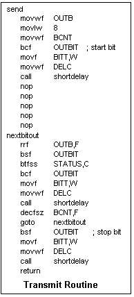
Write subroutines for transmitting and receiving bytes. Use #define statements to specify the pins used, so they will be easy to change. These routines can be used on any MCU, but should be assembled for the proper processor and the proper symbols should be used (i.e., PORTC in place of GPIO, for example). The transmitting routine is shown at the left. It is called with the byte to be transmitted in W. BITT is the bit time byte, 0x31. DELC is decremented in the shortdelay routine. OUTBIT is defined as GPIO,4 in my program. Note that the register bytes are bank-independent in these small processors, but that is not important here.
Write a main program that configures and initializes the processor and makes it easy to send the four bytes to the display. I made the MCU display "C1A0" on the display, which is a hexadecimal word as well as the Italian for "hello". Before loading the program, it was used with MPSIM to check the timing with Stopwatch. Remember to delay a short while for the display to initialize when it is turned on before data is sent to it. Also remember to load OSCCAL with the calibration byte at 3FF, as shown in the assembly template.
Note that we use TTL levels, not the bipolar levels of the RS-232 specification, which is the basic specification for asynchronous links.
Further Possibilities
An asynchronous link is generally full-duplex, in which data can be transmitted on one line and received on another at the same time. A UART can handle simultaneous transmission and reception, but an MCU can only do one or the other at the same time, so a half-duplex link is appropriate, in which transmission is in one direction at a time. In this case a single data wire can be used, with a pull-up resistor to create a high or logic 1 level when transmitters at both ends of the wire are in Hi-Z states, as in the Maxim-Dallas one-wire link. Instead of controlling an output bit, the bit in the TRISIO register is set to release the bus into a 1-state, and is cleared to pull the bus low with a permanent clear bit in the GPIO register. In this way, the device at either end can transmit while the other receives. In fact, this link will work to transmit data to an asynchronous receiver in the usual way with no modifications.
A link may require handshaking signals. In general, two are sufficient, one controlled by each system. They may normally be high. When a system wishes to transmit, it pulls its handshaking signal low. The other system, noting this, prepares to receive and pulls its handshaking signal low in reply. The signals may be called request to send, RTS, and clear to send, CTS. when the transmission is complete, the sending system pulls its handshaking signal high. The receiving system, noting this, pulls its high in response. Neither system transmits unless its CTS signal is low, so the handshaking prevents collisions. Where the transmission is always in the same direction, and the receiver is always ready, handshaking is not necessary.
References
Consult the information on the EUSART of the 16F690, or the mid-range user's manual, for the usual facilities for asynchronous communication.
Return to Electronics Index
Composed by J. B. Calvert
Created 7 October 2010
Last revised