Sample and Hold
In the page on Analog-to-Digital conversion, the importance of using a sample-and-hold circuit with a successive-approximation A/D converter (like the ADC0804) was emphasized. In fact, if the input voltage to be digitized is varying, a sample-and-hold circuit is mandatory. A/D converters with more precision cannot give their advertised accuracy without a sample-and-hold. In this page, the principle of a sample-and-hold circuit is explained and illustrated, and the practical use of the LF398 monolithic sample-and-hold circuit is described. We also measure the leakage currents that exist in these circuits.
What happens is this: when the S/H is in the "sample" state, with the control voltage above 1.4 V, the voltage at the input appears at the output, and varies simultaneously. A S/H presents a very high input impedance, and its bandwidth is considerable. When the control is changed to "hold," below 1.4 V, the sampled voltage is held on a hold capacitor and the output voltage is frozen at that point. There is a settling time after the hold command until the output is within 1 mV of its steady value. For the LF398, this is about 0.8 μs. After the hold command, the aperture time is the time after which changes of the input voltage no longer affect the output voltage. For the LF398, it is 150-200 ns. The acquisition time is the time for the internal nodes to settle, and the output to be within, say, 0.1% of its final value, when a 10 V step is made at the input. The acquisition time depends on the size of the hold capacitor. For the LF398, with a 0.01 μF hold capacitor, it is about 20 μs. Times from the hold command are measured from the 1.4 V point of the control waveform.
Even if the times are taken into account, the accuracy of the output depends on several more parameters. First, the S/H acts like a unity-gain buffer, and its gain may vary slightly from 1. This gain error is less than 0.01% maximum at 25°C. Secondly, there is a finite jump in the output voltage called the hold step when the hold command is issued. For a hold capacitor of 0.01 μF, this is 0.5 mV typically, 2.5 mV maximum for the LF398. Finally, there is droop as the hold capacitor voltage declines steadily in the "hold" state. This droop is caused mainly by a constant leakage current, and can be predicted fairly well, so that corrections can be made for it if desired. All of this should convince you that it is a challenging task to design a good S/H circuit.
Selection of the hold capacitor is an important matter. The larger the hold capacitance, the smaller is the droop. The smaller the hold capacitor, the more quickly it can be charged and the smaller the acquisition time. There is, therefore, a tradeoff in selection of hold capacitor size. For most normal uses, a value of 0.01 μF is satisfactory, and values in the range 1 nF to 1 μF are usual. The type of capacitor used is important. It is obvious that the capacitor should have small leakage, so all electrolytics, whether aluminum or tantalum, are excluded. The next most important characteristic is "dielectric absorption" or hysteresis in the dielectric constant. This means that the voltage is not a single valued function of the charge on the capacitor, as it should be for a S/H circuit. The capacitor voltage changes as the dielectric "relaxes," as well as when charge is supplied or taken away. Ceramic capacitors are unusable because of their high hysteresis, greater than 1% of the voltage on them. Otherwise excellent mica and polycarbonate capacitors have less hysteresis, but still too much for a S/H. The three dielectrics that are suitable for an accurate S/H circuit are polypropylene, polystyrene and Teflon, roughly in that order. Polypropylene has the least hysteresis of all, and is the best choice for a hold capacitor, but any of the three will give adequate results.
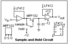 A pretty good S/H can be put together from discrete components, as shown at the right. A more practical discrete sample-and-hold circuit is given in Signal Switching. The LF412 is a dual FET-input op-amp with very small input bias currents. Bipolar op-amps are not suitable, because the input base currents are too large. The circuit is basically two unity-gain buffers, with a hold capacitor between them, and a switch to disconnect the input. The switch is made from a JFET, which does very well. To sample, the gate is connected to the drain (or the source), and to hold, the gate is connected to -V. This is not a very convenient way to control the JFET, but it works for a demonstration. One could also use a MOSFET, such as one of those in the CD4007, but I did not do it here. Control of the MOSFET would be simpler, since the gate could just be connected to +V to sample and -V to hold, because it is isolated. Apply an input voltage with a potentiometer, and watch the output voltage track it while the gate is connected to the drain. When the gate is connected to -V, the output will freeze, and you will note that it droops slowly but steadily. Measure the time required for it to fall by 1 V. I found about 5 minutes, so the droop rate is 3.3 mV/s. This corresponds to a leakage current of only 33 pA, an excellent result.
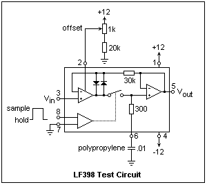 The LF398 is connected as shown at the left. The similarity to our test circuit is obvious. One change is that the feedback loop is extended from input to output. This requires the opposed diodes that "catch" the output of the first op-amp when the feedback loop is broken in the "hold" state. These diodes then require the 30k resistor to avoid overloading the output amplifier. A 300Ω resistor is put in the hold capacitor lead, probably for stability and limiting the charging current. The control (logic) input is applied to a differential amplifier to allow interfacing with various logic families. For us, we want to refer the logic to ground by connecting pin 7 to ground, and apply a positive input to pin 8 for the sample state. The transition voltage is 1.4 V in this case, so any LS or HC output can control the chip. The supply voltage should be within ±5 V and ±18 V. For the test, I used ±12 V. The input resistance of the LF398 is 1010 Ω, a nicely high value, while the output resistance is less than 4 Ω (typically 0.5 Ω). The rise rate of the logic control should be greater than 1.0 V/μs, or the hold step will be excessive. LS or HC logic will do very well. Buffer a slow signal with an LS14. In the test, I used my debounced pushbutton for the logic signal, choosing the normally-low output.
Apply about 5.00 V (say) and hold it. Record the time at the start, and at every even volt as the output voltage droops. I found that it took 28 minutes to decline to 0.00 V. The voltage kept on decreasing, until it reached some internal saturation value at -10.76 V. If you plot the output voltage versus time, you will find a straight line with a slope of -3.0 mV/s. This demonstrates that the droop is caused by a constant leakage current, and is not an exponential RC decay. The leakage current is found to be 30 pA. The specifications of the LF398 allow it to be up to 200 pA. Note that we did not do much worse than this with our discrete circuit. The LF398 is much easier to control, however, and is optimized as a S/H. If you need better specs, there are the more expensive LF298 and LF198 (which mainly give an extended temperature range), and the LF398A, with tightened specs. The LF398 is, however, an excellent circuit suitable for most peaceful requirements.
You should have no trouble now in applying the LF398 to a computer-controlled A/D converter. You will only need one extra logic control output, to command the S/H circuit to hold before triggering a conversion.
Return to Electronics Index
Composed by J. B. Calvert
Created 29 July 2002
Last revised 30 July 2002